
Global high-mix volume high-speed PCBA manufacturer
9:00 -18:00, Mon. - Fri. (GMT+8)
9:00 -12:00, Sat. (GMT+8)
(Except Chinese public holidays)





HomePage > Blog > Knowledge Base > How Sensor PCB Assembly Affects Measurement Accuracy
Table of Contents
1. What Determines Measurement Accuracy in Sensor PCB Assembly
2. Where Accuracy Can Be Lost During Sensor PCB Assembly
3. Different Sensor Applications Need Different PCB Assembly Controls
4. How Sensor PCB Functional Testing Verifies Performance
5. Sensor PCBA Prototype Assembly: From Accurate Prototypes to Production
6. Choosing a Sensor PCB Assembly Manufacturer
Even minor fluctuations can affect the operation of the system, whether it involves industrial automation, medical equipment, IoT solutions, robots, drones, or environmental monitoring. Poor sensor PCB assembly can produce electrical interference, heat problems, mechanical stress, or unreliable contacts that cannot be easily detected with simple inspection. Selecting the proper sensor PCB assembly can help manufacturers mitigate these risks at each stage of the manufacturing process.
In this guide, we will examine the impact of precision sensor PCB assembly on measurement accuracy, sources of errors during production, the different requirements for PCB assembly of various sensor types, and the criteria for selecting a sensor PCB assembly manufacturer.
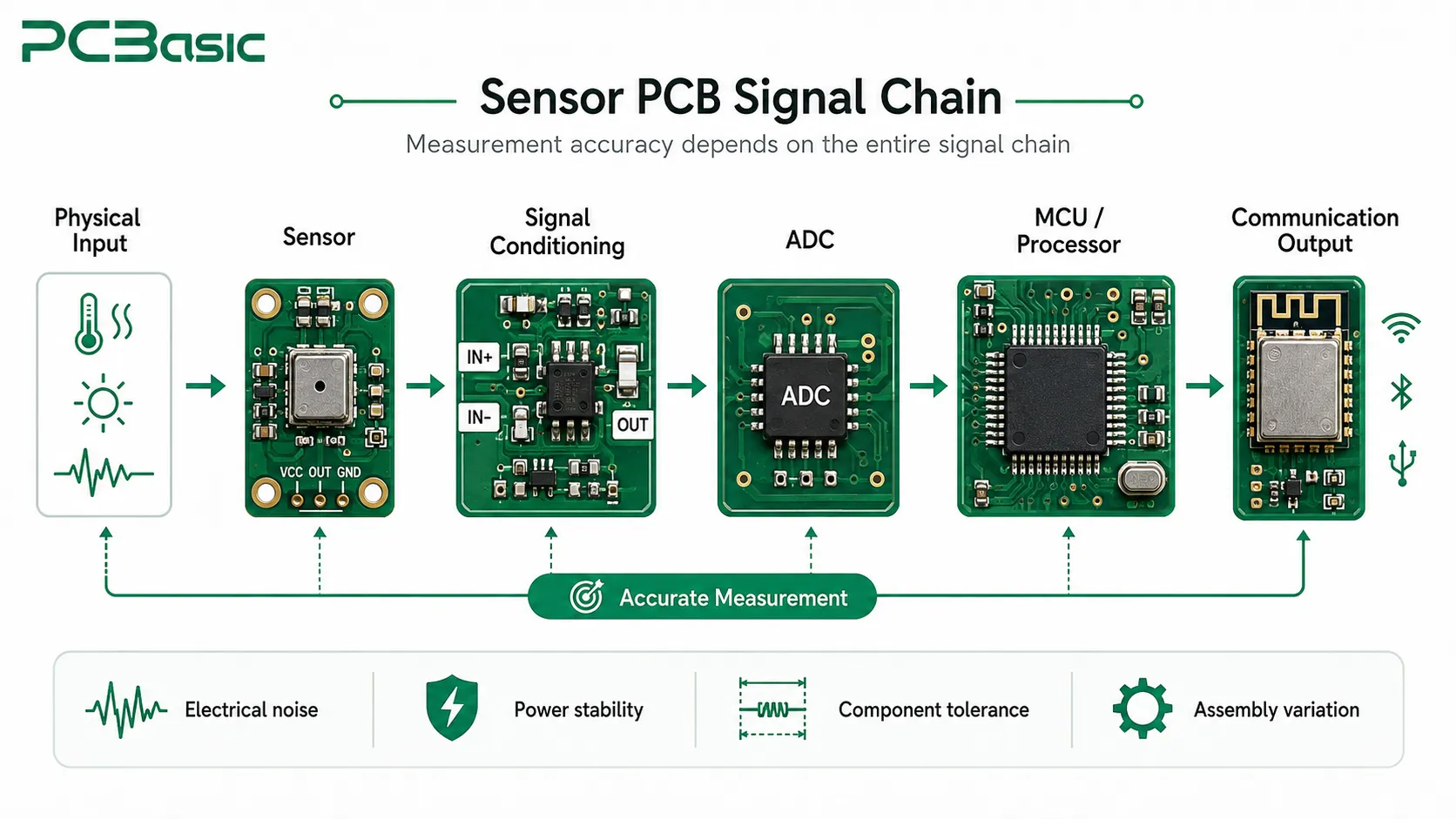
The accuracy of measurements depends on the entire electronic signal chain. The sensor alone is just one component of the system. The PCB design determines the electrical environment required for the sensor, while PCB assembly must consistently reproduce this design through precise component placement, reliable solder joints, and controlled manufacturing processes. Even with a well-designed sensor circuit, its performance may still deteriorate due to assembly variations, poor connections, contamination, excessive heat exposure, or mechanical stress.
The usual elements of the sensor system include the sensor component itself, signal conditioning, amplification, filtering, voltage regulation, conversion, control, and interface devices. Every step can impact the signal.
The sensor converts the physical phenomenon into an electrical signal. The phenomenon that serves as the input depends on the application. The resultant signal is then passed through the PCB before being transmitted to the processor or interface. At the design stage, grounding, signal routing, filtering, and power distribution determine how well the circuit protects the sensor signal from interference. During assembly, incorrect components, poor solder joints, contamination, or process variation can prevent the finished PCBA from achieving the intended performance.
This highlights how vital consistency in PCB assembly and layout is. Consistency in the assembly of a sensor PCB means that the intended electrical properties of the design are maintained from the sensor interface up to the output.
A properly powered sensor PCB is not necessarily an accurate one. Incorrect placement or excessive positional variation can affect thermal coupling, mechanical stress, parasitic effects, or optical alignment in sensitive sensor designs. Another instance is when the soldering is done inconsistently, leading to variable resistance. Overheating can distort the temperature-sensitive parts.
These issues will not be detected with a basic power-up test. Precision sensor PCB assembly therefore requires more comprehensive electrical and functional verification. It is not just about building a working PCBA, but a PCBA that functions consistently within a certain measurement range.
Some factors that influence sensor accuracy originate in PCB design rather than assembly. Layout, grounding, routing, filtering, and component location are established during the design stage, while assembly is responsible for reproducing that design consistently and avoiding additional manufacturing variation. Several stages of sensor PCB assembly can still affect final measurement performance.
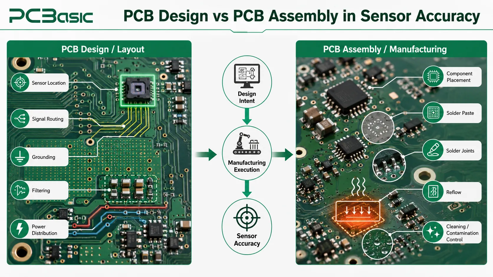
PCB layout defines where sensitive components should be placed, while assembly must reproduce those positions and orientations accurately. Assembly risks include placement errors, solder-paste variation, solder defects, and unsuitable reflow conditions. Sensitive sensors, amplifiers, capacitors, resistors, converters, and processors have to be placed considering the design of the PCB.
The issue of solder paste printing has to be considered. Variations in the amount of paste used may cause insufficient solder joints, solder bridging, and unreliable connections. When the board undergoes the reflow soldering stage, the temperatures have to comply with the requirements of the components and solder materials. An unsuitable reflow profile—such as insufficient peak temperature or time above liquidus—can cause poor wetting or incomplete reflow, while excessive thermal exposure may damage components or the PCB.
Thus, a properly controlled process of assembling an SMT sensor PCB has to control the following parameters:
• Solder paste deposition
• Component placement accuracy
• Component orientation
• Reflow temperature profile
• Solder joint quality
• PCB cleanliness
• Inspection results
Many analog sensors handle low-level signals, and thus are prone to being affected by electrical noise. Common sources of interference include switching power supplies, motors, wireless communication modules, and high-speed digital circuits. If sensitive analog circuits are close to these noise sources, or if the power supply itself has significant fluctuations, it can lead to unstable sensor output.
In this regard, it is necessary to distinguish the roles of PCB design and PCB assembly. During the design stage, grounding, signal routing, filtering, power distribution, and the isolation methods between sensitive analog circuits and noise sources determine the circuit's ability to resist interference.
PCB assembly cannot compensate for a design that already has signal integrity issues, but the manufacturing process must accurately implement the original design. For example, using the correct components, ensuring accurate placement and orientation, forming reliable solder joints, and avoiding contamination or other process deviations.
Therefore, the final performance of the sensor depends not only on whether the initial design is reasonable, but also on whether the design can be stably and accurately implemented during the production process.
Another key parameter is temperature. At the PCB design stage, temperature-sensitive sensors should be positioned with consideration for nearby processors, regulators, LEDs, and other heat-generating components. During assembly, excessive thermal exposure, soldering variation, board warpage, or placement errors can introduce additional thermal or mechanical effects. In the case of temperature sensor PCB assembly, this may be an issue due to the fact that the PCB itself will influence the thermal environment of the measurement.
Mechanical sensitivity should first be considered in PCB and mechanical design, especially for MEMS and pressure sensors. During production, board handling, depanelization, connector insertion, soldering, and final assembly can introduce additional stress that affects sensitive devices.
Contamination is primarily a manufacturing and assembly concern. Flux residue, dust, moisture, fingerprints, or cleaning residues can change surface resistance, interfere with exposed sensing areas, or affect optical components. Hence, quality sensor PCB manufacturing and assembly processes should take into account not only the correct placement of electronic components but also other factors.
There is no universal manufacturing process that will work the same for all types of sensors. The assembly process of a pressure sensor PCB is not the same as that of an optical sensor PCB. Likewise, there can be certain differences between assembly processes for an IoT sensor PCB and an industrial monitoring PCB. This knowledge of the application helps the manufacturer choose the appropriate assembly, inspection, and test methods.
Pressure sensors work by translating physical pressure into an electrical signal. The circuits of the pressure sensors can have signal conditioning stages. Therefore, in the process of assembling pressure sensor PCBs, all these factors should be taken into consideration.
Temperature sensor PCB assembly requires coordination between PCB layout and manufacturing. The layout should place the sensor in a reasonable position relative to nearby heat-generating components, and during the assembly process, this position must be maintained while controlling thermal stress and mechanical stress. For environmental temperature measurement, the heat generated by the PCB itself may cause measurement values to deviate.
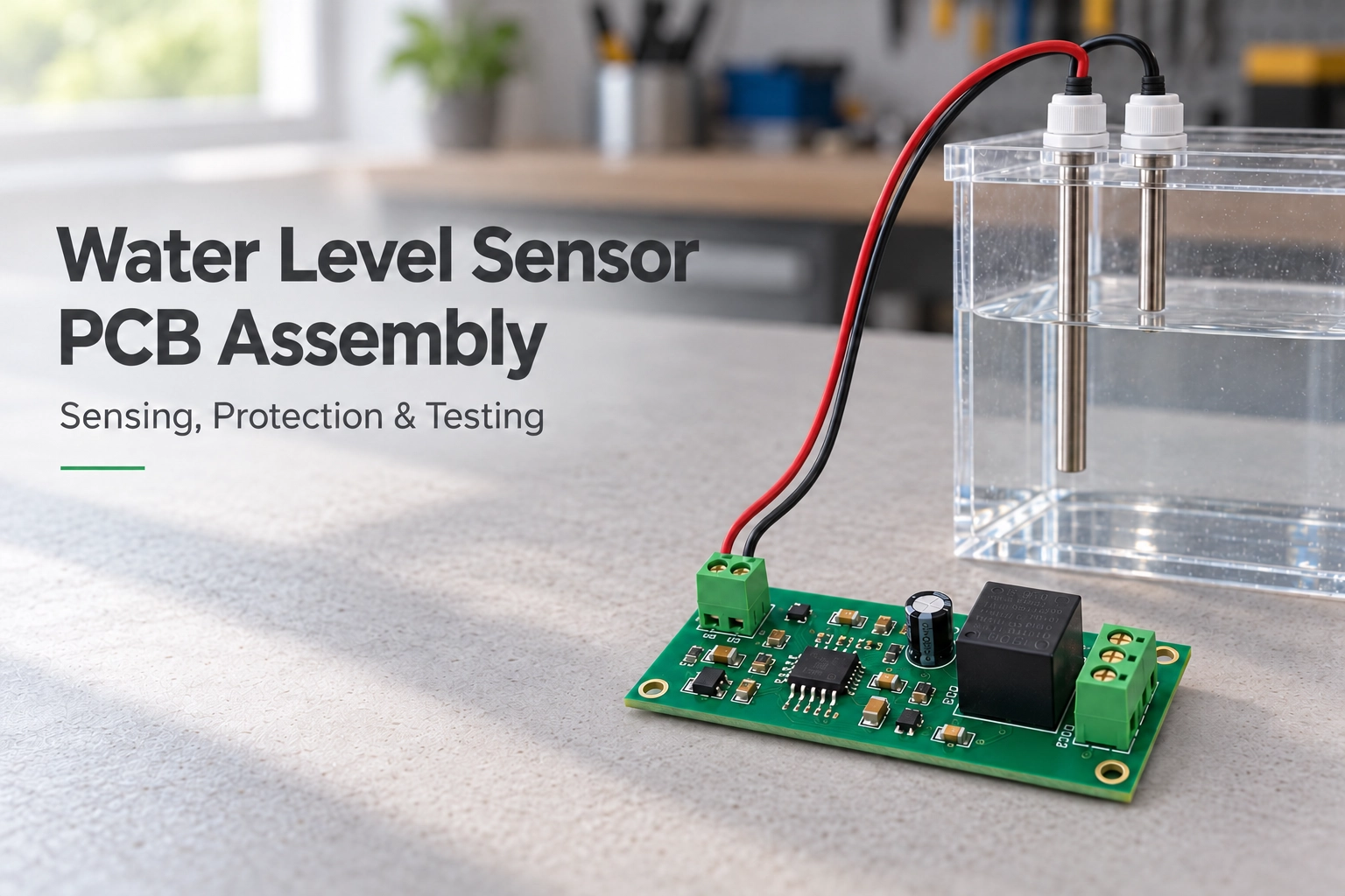
In the case of a water leak sensor PCB assembly, moisture protection and electrical isolation become critical, but exposed sensing areas should remain uncovered where required by the sensor design. The cleanliness of the PCB, component selection, protective coating, or enclosure, and the environment need to be considered.

Optical systems that use emitters and receivers—such as reflective, proximity, or encoder designs—may require precise alignment between the light source, optical path, and detector. As a result, an optical sensor PCB assembly has to be precise and consider electrical and optical interference.
Capacitive proximity and touch sensor circuits are also prone to interference from the conductive materials in the surroundings and electrical noise in the environment. Assembly consistency is vital in making sure that the boards manufactured in various batches perform similarly.
An IoT sensor PCB assembly could incorporate the functionality of many sensors with wireless communication and processors. This leads to an electrically complicated setup. There are other issues presented by the application involving robots and drones since the sensor board will be subjected to vibration, motion, and varying temperatures.
Industrial sensor PCB assembly may need to maintain stable performance under vibration, temperature variation, electrical noise, or other demanding operating conditions. For applications with these requirements, PCBasic provides SMT and mixed-technology assembly, functional testing, and engineering support for industrial sensor PCBs.
Inspection helps detect manufacturing faults, but it does not mean that inspection itself ensures proper functioning of the sensor board in actual operating conditions. That is the reason why functional testing of the sensor board is very important in the production process.
There are various stages of inspection in a modern PCB assembly quality control system. It may depend on the design and manufacturing process and could consist of:
• Visual inspection
• Solder paste inspection
• Automated Optical Inspection (AOI)
• X-ray inspection
• In-Circuit Testing (ICT)
• Functional Testing (FCT)
• Final quality inspection
According to PCBasic, its PCBAs are checked and tested via several stages: AOI, X-ray inspection, ICT, functional testing, and final testing. These methods detect different types of defects: AOI checks visible component and soldering issues, X-ray reveals hidden solder-joint defects, ICT identifies electrical faults such as opens and shorts, and FCT verifies the board's intended functions.
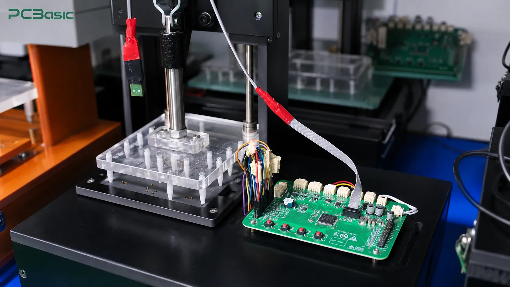
In the case of sensor PCB functional testing, one should reproduce operating conditions. For example:
• The temperature sensor can be tested at various temperature points.
• A pressure sensor can be tested by applying controlled pressure points and comparing the electrical output with the expected response.
• Proximity sensors can be analyzed through controlled conditions of detection.
• The IoT sensor board can be tested for sensor response, processing, and communications functionality.
This type of test verifies that the circuit functions in accordance with its requirements under the tested conditions. PCBasic can perform functional testing according to customer-defined procedures. For tests requiring specialized fixtures, reference equipment, or dedicated hardware, these requirements should be confirmed in advance.
Functional testing and calibration must not be confused. Functional testing tests if the board functions properly. Calibration tests the output of the sensor with respect to its reference values to see if corrections are necessary. There is a possibility that the board may pass in functional testing, but it needs to be calibrated. The process of calibration varies depending on the type of sensor, its accuracy, and the intended purpose.
It takes more than just ordering larger quantities when moving to volume manufacturing. Sensor PCBA prototype assembly can be a good way for engineers to pinpoint any problems that could arise before starting full-scale production. Prototypes provide the opportunity for evaluation of component availability, positioning, soldering, sensor reaction, testing process, heat resistance, and system performance.
PCBasic offers a wide range of services related to prototype PCB assembly, helping to test and refine sensors before launching them into mass production.
During the process of sensor PCBA prototype assembly, one needs to examine:
• Sensor response
• Component selection
• PCB layout
• Signal integrity
• Power stability
• Thermal behavior
• Mechanical requirements
• Assembly quality
• Functional testing
• Calibration requirements
It will help to avoid costly changes in design further.
Once the design reaches the manufacturing stage, however, consistency is key. A reliable sensor PCB assembly manufacturer should have control processes for solder paste printing, automatic placement, reflow, inspection, testing, parts handling, and tracking.
PCBasic uses digital manufacturing and process management technologies in order to assist in production monitoring and quality management.
When it comes to complex PCBs, mixed technology sensor PCB assembly may be used where through-hole and surface mount technologies are combined. Such a combination will be able to accommodate the requirements for surface-mount devices and through-hole devices as well. PCBasic offers SMT, THT, and mixed PCB assembly technologies.
Choosing a vendor by looking at just the price of assembly may cause difficulties in the future. When choosing sensor PCB assembly services, one should take into account manufacturing capabilities, testing capabilities, quality management, engineering support, and production scalability.
A complete RFQ should include the required PCB assembly files, such as:
• PCB Gerber files
• Bill of Materials (BOM)
• Pick-and-place files
• Assembly drawings
• Component specifications
• Sensor operating range
• Required tolerances
• Testing requirements
• Calibration requirements
• Environmental requirements
• Prototype quantity
• Production quantity
• Quality standards
• Packaging requirements
Buyers should also ask if the vendor can help with the project, not only during the development but also after it. Is the manufacturer able to move the design into the volume production phase? Is it capable of doing functional testing? Is it able to assist with component procurement? Can it support SMT and mixed-technology assembly? These questions will help identify a sensor PCBA manufacturer who can provide full support throughout the product life cycle.

In the case of sensor products, assembly quality is one important factor affecting the reliability of the finished electronic product. PCBasic offers PCB assembly services, including SMT, THT, mixed assembly, prototype assembly, turnkey assembly, and functional testing.
PCBasic also provides AOI, X-ray, ICT, and FCT in order to help detect assembly defects and verify board performance. If the projects require fast development, then PCBasic supports prototype assembly as well as scalable production. These capabilities can support sensor products from prototype validation through mass production.
Accuracy in measurement does not only depend on the sensor part, but on the whole sensing system. Aspects such as signal integrity, power regulation, heat dissipation, reliability, and the performance of the assembled board can be affected by the PCB assembly quality of the sensors. The positioning, SMT soldering, reflow, inspection, and functional testing processes play a critical role in the final result.
There are special manufacturing controls for different types of applications. Examples include pressure sensor PCB assembly, temperature sensor PCB assembly, optical sensor PCB assembly, water leak sensor PCB assembly, IoT sensor PCB assembly, and medical sensor PCB assembly. The most effective practice will be validation of the design while performing sensor PCBA prototype assembly and proper testing/calibration procedures during mass production.
Are you in search of dependable sensor PCB assembly services? We can support your project from prototype development to mass production through SMT, mixed-technology assembly, inspection, and functional testing. Get a quote from PCBasic and discuss your PCB assembly requirements with our experts.
Q1: What is a sensor PCB assembly?
A1: It involves the installation and soldering of the electronic components on a PCB, which receives, processes, and transmits signals created by the sensors.
Q2: How does sensor PCB assembly affect measurement accuracy?
A2: Factors such as component positioning, solder joints, reflow, power source, electrical noise, temperature, and contamination could all have an impact on the sensor circuit operation and measurements.
Q3: Why is sensor PCB functional testing important?
A3: Sensor PCB functional testing is aimed at making sure that the assembled board works in line with its specified electrical functionality, and not just its ability to power up.
Q4: What is the difference between sensor PCB testing and calibration?
A4: Testing ensures that the PCB and the sensors work as intended. Calibration compares the sensor output with a known or traceable reference under defined conditions.
Q5: What should I look for in a sensor PCB assembly manufacturer?
A5: Consider such capabilities as SMT and mixed technology capability, automated testing, X-ray testing, electrical testing, functional testing, prototyping capability, component sourcing, quality certifications, and scalability from prototypes to manufacture.

Assembly Enquiry
Instant Quote


Phone contact

+86-755-27218592
In addition, we've prepared a Help Center. We recommend checking it before reaching out, as your question and its answer may already be clearly explained there.
Wechat Support

In addition, we've prepared a Help Center. We recommend checking it before reaching out, as your question and its answer may already be clearly explained there.
WhatsApp Support

In addition, we've prepared a Help Center. We recommend checking it before reaching out, as your question and its answer may already be clearly explained there.
