Global high-mix volume high-speed PCBA manufacturer
9:00 -18:00, Mon. - Fri. (GMT+8)
9:00 -12:00, Sat. (GMT+8)
(Except Chinese public holidays)
Global high-mix volume high-speed PCBA manufacturer
9:00 -18:00, Mon. - Fri. (GMT+8)
9:00 -12:00, Sat. (GMT+8)
(Except Chinese public holidays)
HomePage > Blog > Knowledge Base > What Is DIP Soldering? A Comprehensive Guide
The reliable electrical connections of almost all electronic devices are inseparable from soldering. Soldering involves using fusible metal alloys (traditionally tin-lead alloys, but now more often lead-free alloys) to fix and connect electronic components to the PCB. The alloy melts when heated and solidifies after cooling, firmly binding the components electrically and mechanically together. It can be said that without soldering, there would be no today's various electronic products, regardless of which industry they belong to.
Different production requirements lead to different soldering processes, such as SMT soldering, DIP soldering, reflow soldering, and wave soldering, etc. And today, what we are going to introduce is DIP soldering. Next, we will elaborate on the relevant content of DIP soldering, including its definition, process, advantages and disadvantages, quality control, and comparison with SMT soldering, etc.
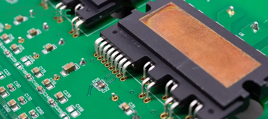
DIP soldering is an assembly process specifically designed for dual in-line package (DIP) components. It is a traditional but very reliable method. The process involves inserting the pins of the DIP packaged component into the pre-drilled through-holes on the PCB and then securing them with solder. This process can be carried out manually or with the help of a DIP soldering machine. In mass production, automatic DIP soldering machines (such as wave soldering machines) are commonly used to increase efficiency.
DIP soldering is a typical through-hole technology. Unlike surface mount technology (SMT) which directly solders components onto the board surface, DIP soldering can provide stronger mechanical bonding force and higher reliability. Nowadays, due to the demand for miniaturization, SMT is used more frequently, but DIP soldering is still indispensable. This is because it has high mechanical strength and can withstand large currents and high voltages. These advantages are indispensable for equipment in fields such as automotive electronics, power equipment, industrial control, aerospace and military. Here is a detailed comparison table between DIP soldering and SMT soldering.
|
Aspect |
DIP Soldering |
SMT Soldering |
|
Component Package Type |
Dual In-line Package (DIP), leads inserted into holes |
Surface Mount Device (SMD), mounted directly on pads |
|
Mounting Method |
Leads are inserted into PCB through-holes and soldered |
Component terminals are soldered directly onto PCB pads |
|
Soldering Process |
Mainly Wave Soldering or manual soldering |
Mainly Reflow Soldering |
|
Solder Joint Location |
Formed on the opposite side of the PCB, high mechanical strength |
Formed between component and pad, small size |
|
Equipment Required |
Wave soldering machine, manual soldering station |
Reflow oven, pick-and-place machine |
|
Circuit Density |
Limited by through-holes, lower routing density |
No through-holes needed, supports high-density routing |
|
Mechanical Strength |
Strong, suitable for large components (capacitors, transformers, connectors) |
Weaker, suitable for small and lightweight components |
|
Application Scenarios |
Power boards, automotive electronics, large industrial equipment |
Smartphones, computers, wearables, high-speed circuits |
|
Main Disadvantages |
Larger space usage, complex routing, lower automation |
Weaker solder joints, prone to defects like tombstoning/bridging, harder to rework |
|
Typical Defects |
Excess solder, cold joints, insufficient solder |
Tombstoning, bridging, cold joints |
|
Advantages |
Strong solder joints, high reliability, good mechanical stress resistance |
Compact size, supports high-density design, excellent for mass automation |
The DIP soldering process is a structured method. The overall process for soldering all DIP components is the same. Below, we will introduce it to you step by step.
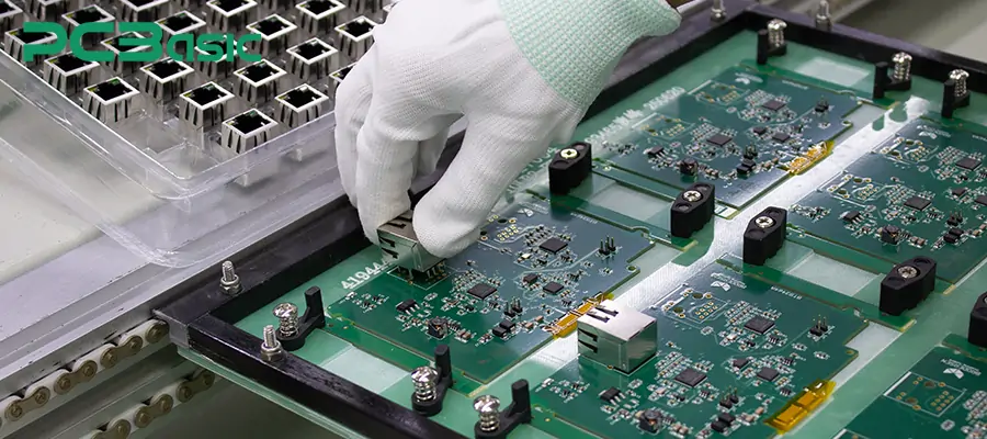
Before starting the DIP soldering process, we must first prepare the PCB and the corresponding components. Then, we need to conduct a corresponding inspection on the circuit board. We must check whether the hole diameters are correct, the coating quality is qualified, and the cleanliness is adequate. This is the first step to ensure the reliability of the subsequent solder joints on the circuit board. The components also need to be inspected. We must check the polarity and orientation of the components, especially for components like ICs, diodes, and electrolytic capacitors. In addition, if it is manual soldering later, then we need to prepare an electric soldering iron, flux, and solder wire; if using a DIP soldering machine, such as wave soldering, for soldering, then we need to set up the flux sprayer, preheater, and tin bath. Finally, but equally important, we must take safety and static protection measures.
After the preparatory work is completed, the component insertion process can be carried out. The correct placement of components is crucial. Components should be inserted into the pre-drilled PCB holes and should be closely attached to the surface of the circuit board to ensure better consistency in the flow of solder. It is also important to note that for some components, their pins need to be pre-formed to match the pitch and be gently bent before soldering to fix the component. During the insertion process, it is best to follow the sequence from lower components to higher ones. This can reduce mechanical stress and shadow effects during the soldering process.
After all the components are inserted, it's time for the soldering process. For prototype production, small batch manufacturing, or repair work, we can perform manual DIP soldering directly. Using a temperature-controlled soldering iron to heat both the pads and the component pins simultaneously, and then adding solder until a smooth and shiny solder joint is formed. This manual soldering method is flexible and precise, but it is slower and requires skilled operators.
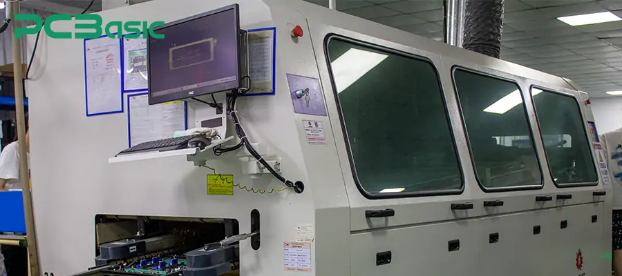
For large-scale assembly, we often choose to use a wave soldering machine. The circuit board will go through three stages: flux coating, preheating, and the contact of the solder wave. As the solder wave melts, it will come into contact with the exposed pins and pads, thereby forming uniform solder joints between the circuit board and the components. This method is the preferred choice for through-hole assembly in large-scale production.
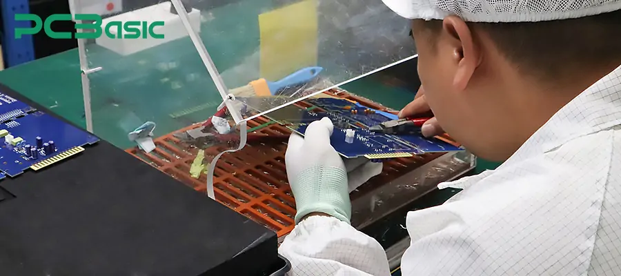
After the soldering is completed, we need to trim the excess component pins to the appropriate length (usually keeping 0.5 - 1.0 mm above the solder joints). This ensures that the produced circuit boards are safer, more reliable and more standardized. Then, depending on the type of flux used, the circuit boards should be cleaned. The water-soluble flux residues can be rinsed with deionized water, and the rosin-based residues can be removed with isopropyl alcohol. Do not forget to clean them, as cleanliness is extremely important. Residues may affect long-term reliability and interfere with subsequent conformal coating and other processes.
The final step is rigorous inspection and quality control. Each solder joint must be evaluated in accordance with the IPC-A-610 standard. Key criteria include smooth solder joints, adequate wetting of pads and pins, sufficient hole filling rate, and absence of common defects such as bridging, cold soldering, or gas pores. For non-compliant solder joints, they can be re-soldered by applying flux for repair to restore reliability.
One of the major advantages of DIP soldering is that the mechanical connection it forms is extremely strong. When the component pins are inserted into the through-holes of the PCB and the soldering is completed, the molten solder will surround the entire pin. This design not only ensures reliable electrical connections for the circuit board, but also enhances its mechanical strength. This advantage makes DIP soldering particularly suitable for products that are frequently operated, easily subject to mechanical impact or vibration.
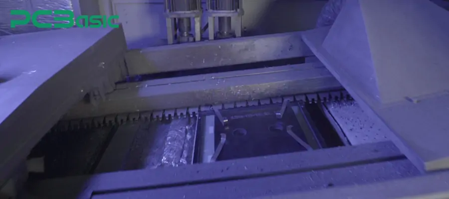
Another important advantage of DIP soldering is that it can withstand greater current and voltage. The contact area between the DIP through-hole solder joints and the component leads is larger, so it can carry higher currents without overheating or aging. Power devices such as transformers, relays, capacitors, and power transistors often use the DIP soldering process for soldering.
In terms of repairability, DIP soldering also has obvious advantages. When maintenance or servicing is needed, ordinary soldering tools (such as soldering irons or desoldering machines) can be used to easily remove and replace the through-hole components. In contrast, surface mount components, especially those with fine pitches or ball grid array packages, require specialized rework equipment and technicians. In comparison, DIP soldering is indeed convenient and economical.
Furthermore, in harsh working environments, DIP-soldered circuit boards can also exhibit extremely high reliability. Due to its larger solder joints and the fixed method of the through-holes, it can effectively resist thermal expansion and contraction, so it is less likely to fail even after repeated heating and cooling cycles.
Although DIP soldering has obvious advantages in terms of reliability and strength, it still has some limitations.
Firstly, the cost of DIP soldering is usually higher. In traditional processes, DIP components usually require manual insertion and soldering, which poses a challenge to production efficiency. Even with the use of automated wave soldering machines or automatic DIP soldering machines, additional dedicated equipment and processes are still needed. While the SMT production line can complete the entire soldering process by machines. For mass production, compared to SMT, the cost of DIP soldering is much higher.
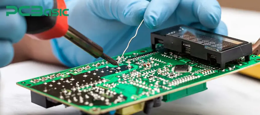
Secondly, DIP components will occupy more PCB space. Because the pins of DIP components need to pass through the circuit board, holes must be drilled for each pin during design. This not only increases the difficulty of PCB routing but also expands the overall board area. Compared to SMT components, DIP soldering cannot achieve high-density wiring and device arrangement within a limited space. In modern electronic products with extremely high requirements for circuit board thinning, this limitation is particularly obvious. This is also the fundamental reason why DIP soldering is gradually being replaced by SMT in the consumer electronics field.
Although SMT soldering is the mainstream in modern electronic manufacturing, DIP soldering is still an indispensable soldering process in many fields that have strict requirements for reliability and mechanical strength.
1. In the automotive electronics field, many modules need to handle large currents and operate in harsh environments for a long time. For example, engine control units (ECUs), power distribution modules, and ignition control systems. These modules must use DIP soldering technology because the DIP soldering method enables the circuit board to have a strong mechanical bonding force and the ability to carry large currents.
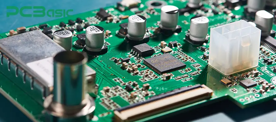
In addition, as mentioned earlier, DIP soldered circuit boards can also exhibit extremely high reliability in harsh environments. This is very important for some modules in automotive electronics. Because during vehicle operation, these modules will undergo intense vibrations and temperature changes, and DIP soldering provides reliability that ensures these critical modules can operate stably for a long time.
2. In the power electronics field, DIP components are the core part, and DIP soldering is undoubtedly indispensable. Components such as transformers, relays, power adapters, and power transistors are usually large in size and require stable electrical paths during operation. And the DIP soldering technology can firmly fix these devices on the circuit board while ensuring that they will not fail due to poor contact in high-current and high-voltage environments.
3. In industrial automation equipment, reliability and durability are crucial. Many control circuit boards, PLCs, motor controllers, and sensor interfaces still use DIP soldering technology. Due to the presence of dust, moisture, and electromagnetic interference in industrial environments, the DIP structure with through-hole solder joints can better resist environmental factors and ensure the long-term stability of the system.
4. In the military and aerospace fields, electronic equipment must remain stable and reliable under extreme conditions. Aircraft, satellites, military radars, and weapon systems all require circuit boards to be able to withstand high temperatures, intense vibrations, shocks, and strong radiation environments. The strong mechanical fixation and stress resistance provided by DIP soldering are among the reasons why it has become a common process in these highly reliable applications.
Not all DIP solders result in secure and reliable solder joints. During the soldering process, in order to ensure the firmness and reliability of the soldered joints, strict quality control measures must be implemented during the production process.
The most typical problems that may occur in DIP soldering include cold solder joints, solder bridging, and insufficient solder.
If these problems occur in high-current devices or critical control modules, serious consequences will ensue. Therefore, to avoid these problems, multiple detection methods need to be adopted for quality control.
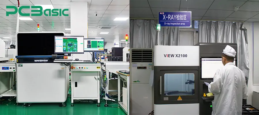
The AOI machine is used to quickly identify surface defects such as missed solders and solder bridging;
The X-Ray inspection machine is used to detect internal problems that are invisible to the naked eye, such as incomplete immersion of pins or voids in the solder joints;
In addition to machine inspections, manual inspection and sampling checks are still indispensable. Multiple detection methods are necessary to ensure the consistency and reliability of the solder joints without any flaws.
In terms of quality standards, DIP soldering needs to follow the IPC-A-610 standard. This standard sets clear requirements for the appearance of solder joints, the degree of wetting, and the control of residues. This standard regulates the manufacturing process of manufacturers and provides reliable quality assurance for customers.
DIP soldering is a traditional process and represents the durability and reliability of soldering in electronic manufacturing. Although SMT soldering technology has facilitated miniaturization and high-speed production, in areas that require mechanical strength, large current carrying capacity, and long-term stability, DIP soldering remains an indispensable solution.
 About PCBasic
Time is money in your projects – and PCBasic gets it. PCBasic is a PCB assembly company that delivers fast, flawless results every time. Our comprehensive PCB assembly services include expert engineering support at every step, ensuring top quality in every board. As a leading PCB assembly manufacturer, we provide a one-stop solution that streamlines your supply chain. Partner with our advanced PCB prototype factory for quick turnarounds and superior results you can trust.

Assembly Enquiry
Instant Quote
Phone contact

+86-755-27218592
In addition, we've prepared a Help Center. We recommend checking it before reaching out, as your question and its answer may already be clearly explained there.
Wechat Support

In addition, we've prepared a Help Center. We recommend checking it before reaching out, as your question and its answer may already be clearly explained there.
WhatsApp Support

In addition, we've prepared a Help Center. We recommend checking it before reaching out, as your question and its answer may already be clearly explained there.