Table of Contents
1. What Gets Packed onto
a Compact Camera Module PCB?
2. When Less Board Space
Creates More Assembly Constraints
3. Building the Camera
Module PCBA Without Losing Process Control
4. High Density Is Only
Useful If the Camera Actually Works
5. Conclusion
6. FAQs
Camera module
components are getting smaller and this has almost become a very obvious trend.
However, even if the board is smaller, the situation
doesn't get any easier. More functions are filled into a smaller space.
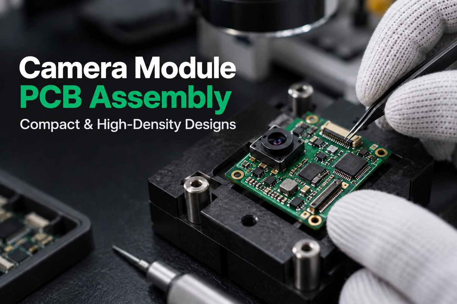
On a small camera module circuit board, you can
find image sensors, chips that process and control the camera, parts that
manage power, resistors, capacitors, connectors, and fast data connections. Some products, in order to adapt to
narrower structural spaces, even add FPC connections, flexible PCB, or rigid-flex
boards. The board isn't big, but it has to manage a lot of
devices and connections.
Because the components are packed more closely
together, the camera
module PCB assembly has higher requirements for solder paste printing, placement
accuracy, cleanliness, and inspection. For a camera module
PCBA, finishing the soldering process is just the beginning. It also needs to
be turned on properly, identify the image sensors, establish communication, and
send the image data consistently.
In this blog,
we will start with the typical structure of a compact camera module PCB and then discuss the challenges that come with a densely packed layout
during assembly. We'll also go over important steps such as SMT, inspection,
and specific camera module testing that need careful attention during the PCB assembly process.
What Gets Packed onto a Compact Camera Module PCB?
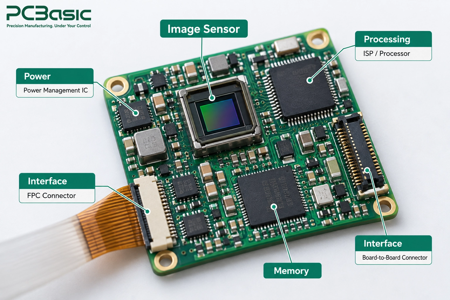
Even if a
compact camera module PCB looks small, it can contain a large number of
components. The image sensor is usually the key component, with many designs
now using CMOS. It may also have an ISP or controller around it, some power
management ICs, memory, a variety of passive components and the interface
circuitry for data transfer.
What are
those parts doing? The light signals fall to the image sensor, the image data
is processed by the ISP / processor, the power circuit providing a constant
voltage to the sensor and the other components. Resistors, capacitors and
inductors seem simple or unimportant, but they are extremely important for
functions like filtering out unwanted signals, preventing electrical noise, and
maintaining signal stability.
The connection part is also very important. Many camera module PCB will
use FPC connectors, board-to-board connectors, or interfaces such as MIPI, USB
to connect with the host system. When the space is particularly tight, flexible
PCBs or rigid-flex PCBs may be used to match the overall structure of
the device.
|
Functional Area
|
Typical Component
|
Assembly Focus
|
|
Imaging
|
CMOS image
sensor
|
Placement
and cleanliness
|
|
Processing &
Control
|
ISP, MCU,
processor
|
Fine-pitch soldering
|
|
Power
|
PMIC, regulators,
passive components
|
High-density
placement
|
|
Interface
|
FPC,
board-to-board connectors
|
Alignment
and solder quality
|
For image
sensor PCB assembly, the real trouble often lies not in the large variety of
components, but in their close proximity. The sensor area needs to be kept
clean and operated carefully. The adjacent fine-pitch ICs, small passive
components and connectors also require that the solder paste printing, mounting
and reflow soldering be stable enough.
The
structures of different products are also different. Some CMOS camera module or
embedded camera module place most of their functions on the same PCB; while in
larger systems, the sensor board, camera control board and the main processor
may be separate.
Therefore, a
small board does not necessarily mean it is easy to manufacture. The more
functions are concentrated, the smaller the error margin left for manufacturing
and assembly in the camera module PCB.

When Less Board Space Creates More Assembly Constraints
The smaller the space on the
board, the more difficult it is to handle differences in the manufacturing
process. In camera module PCB assembly, there's often a lot of small parts like
fine-pitch ICs, tiny passive components, connectors, and circuits related to
the sensor packed into a very small space. Even a small mistake in the earlier
steps can become bigger problems later on.
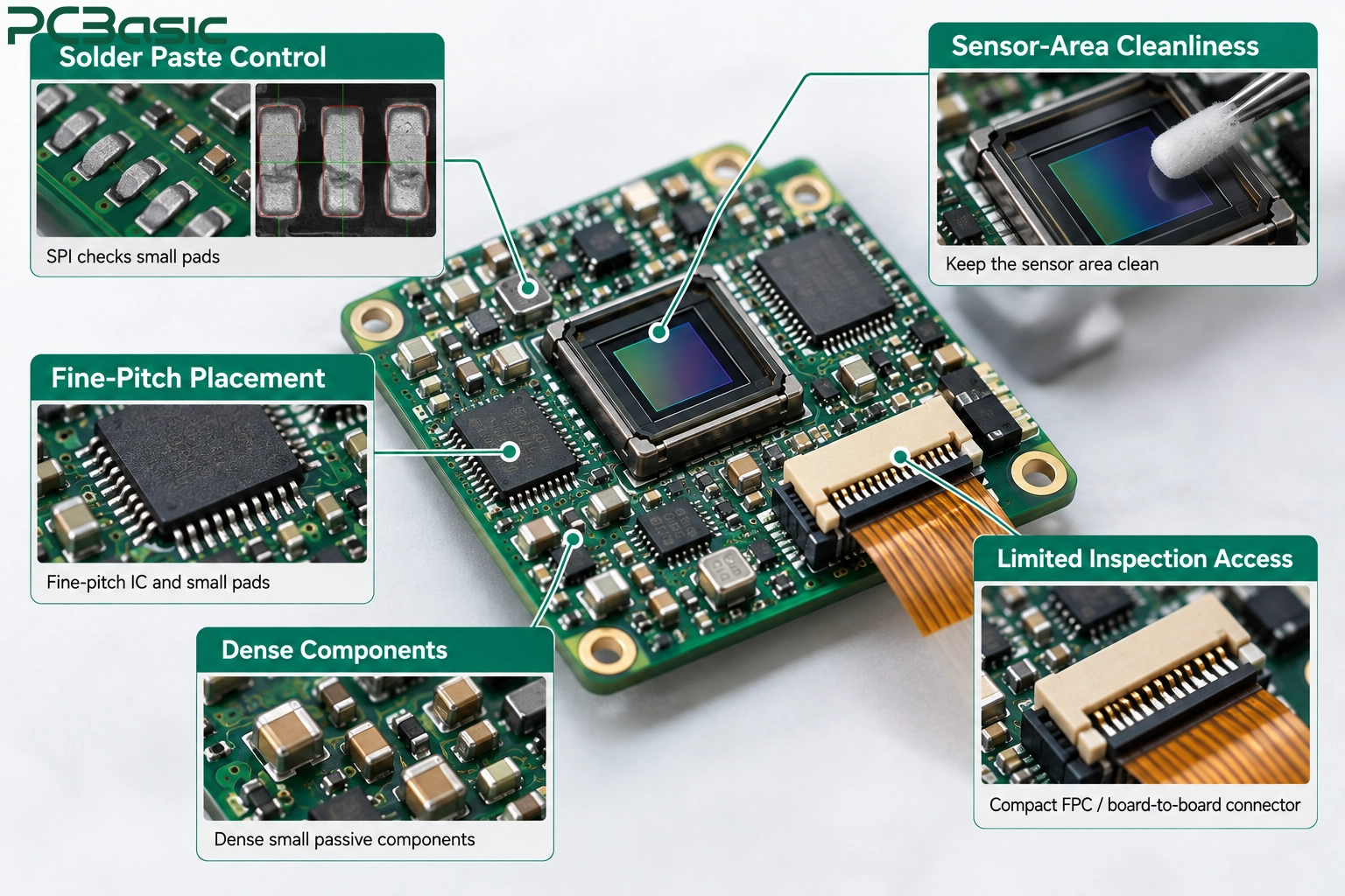
There are several areas that need particular
attention:
• Solder paste control: With smaller pads
and tighter spacing, even a little more or less solder paste can cause
problems. In fine-pitch PCB assembly, we usually check the volume, area,
height, and position of the solder paste through SPI to identify any
abnormalities before component placement.
• Component placement: A compact camera
PCBA often places small passive components near the image sensor, processor,
power circuit, or FPC connector. Therefore, the placement accuracy, component
orientation, and component package identification all need to be maintained
consistently.
• Cleanliness of the sensor area: Image
sensor PCB assembly is more sensitive to dust, particles, and residues. Why is
this? Some boards may test as electrically good, but the contamination problem
only appears after integration into the full optical system.
• Inspection access: The tighter the
component placement, the less room there is for AOI or manual inspection. Some
solder joints may be hidden in components’ bottom, so the inspection method
cannot be generalized but should be selected according to the packaging type
and PCB structure.
This is why high-density PCB assembly cannot
focus on only one aspect. Solder paste printing, placement, reflow soldering,
inspection and testing all have to work seamlessly together. The whole process
should be consistent, so that the quality of the final product can be better
controlled.
Building the Camera Module PCBA Without Losing Process Control
A reliable camera PCB assembly process actually begins before the solder
paste printing. We usually start by checking the BOM, PCB data, packaging
information, component polarity, and placement files. Why is this necessary?
Because many problems, if not detected earlier and addressed after moving to
the SMT line, will result in higher costs and longer processing times. DFM
review can also identify issues such as too-small component spacing,
inappropriate pads, difficult connector locations, or problems that make
subsequent inspection inconvenient.
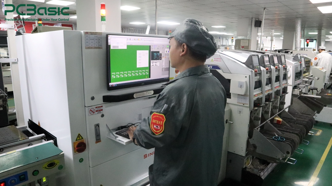
For most camera module PCB assembly projects,
the SMT process is not complex:
Solder paste printing → SPI → Component placement → Reflow soldering → AOI
The real challenge is not the process itself,
but ensuring stability at every step.
For example, SPI can identify issues such as
solder paste volume, position, or printing problems before the placement of ICs
with fine pitch and image sensors. Next, the placement equipment must ensure
accurate component positions and orientations, especially in high-density
areas, small connectors, and around sensors. After reflow soldering, AOI is
responsible for inspecting visible placement and soldering issues. If the
camera PCBA uses hidden solder points packaging, we will decide whether to add
X-Ray inspection based on the packaging type and quality requirements.
Of course, SMT is not everything. Incoming
material inspection, first article confirmation, cleaning or cleanliness
control, programming, and functional testing may all be added to the entire
production process based on project requirements.
At PCBasic, fine-pitch PCB assembly can be
controlled by combining SPI, AOI, 3D X-Ray, IQC/FAI, material traceability, and PCBA functional testing. The purpose of this is
straightforward: to ensure that the process for compact camera module PCBs
remains consistent from the first prototype to subsequent mass production,
without having to rebuild the process repeatedly.
High Density Is Only Useful If the Camera Actually Works
A high-density camera PCB assembly may look fine from the outside, but
it doesn't mean it will work properly once installed in the device. When
actually assembling the board, we often see this kind of situation: the solder
joints may look normal, but as soon as the power is turned on, the sensor
doesn't activate; or the interface can be connected, but the image data is
unstable.
Therefore, when we do camera module testing, we
don't just focus on the solder joints. For a camera module PCBA, what's more
crucial is whether it can run normally after being placed in the system.
Whether the power supply is stable, whether the sensor can recognize, and
whether the data can be transmitted normally - these issues can easily be
exposed when the system is powered on.
For embedded camera modules that need to work
for a long time, we also need to look beyond short-term operation. Running for
a short period of time does not mean it will be stable in the future. Connectors,
power supply, cleanliness around the sensor area, and even the state after
long-term operation can all affect the final performance.
However, it should also be noted that:
completing the electronic functional test of the camera module PCB assembly
does not mean that the entire optical system has been calibrated. Functions
such as focusing, lens position, and image quality calibration usually require separate
equipment and processes.

Conclusion
A smaller camera circuit board does not mean it is easier to
manufacture. As more functions are concentrated into a more limited space, the
real challenge lies in how to ensure that the entire assembly process remains
consistent from the first prototypes to subsequent mass production.
For camera module PCB assembly, ultimately, it
boils down to just one question: This board not only needs to pass the
inspections on the production line, but also, after being installed in the
complete camera system, can it operate stably.
PCBasic can provide support for camera PCB
assembly projects, including PCB
manufacturing,
component sourcing, inspection, programming, and functional testing, helping
customers smoothly transition from prototype verification to stable and
repeatable mass production. If you are developing camera modules or embedded
vision products, you can send Gerber, BOM, placement files, and test
requirements to PCBasic.
We can assist you with DFM review and provide PCB assembly quotations.
FAQs
Q1: What
is camera module PCB assembly?
Camera module
PCB assembly is the process of mounting and soldering image sensors, control
ICs, power components, connectors, and other parts onto a camera module PCB.
The finished camera module PCBA may work as a complete camera board or connect
to other processing hardware.
Q2: Why is
image sensor PCB assembly challenging?
Image sensor
PCB assembly combines normal SMT requirements with tighter control of
placement, solder paste, and cleanliness. As camera PCBA designs become
smaller, fine-pitch PCB assembly and careful inspection become more important.
Q3: How is
a camera module PCBA tested?
Camera module
testing may include electrical checks, programming, interface communication,
sensor startup, and image-data verification. The exact test plan depends on the
CMOS camera module design and project requirements.