Today, with the rapid development of electronic manufacturing,
PCB inspection is becoming increasingly important. Printed circuit boards (PCBs)
are core components of electronic products, such as smartphones, medical
devices, automotive electronics, and aviation systems. The performance of a PCB
is directly related to the functionality, safety and stability of the entire
product. Even a very small defect can lead to equipment failure, quality
problems, and even cause serious economic losses.
To ensure the reliability of each PCB,
manufacturers need to carry out strict PCB inspections during the design,
production and assembly stages. By using reasonable PCB quality control
methods, following industry standards, and being equipped with advanced circuit
board inspection equipment, companies can effectively reduce defects, lower
rework costs, and enhance the overall PCB quality, thereby strengthening
customer trust and market competitiveness.
This blog will introduce several
commonly used PCB quality control methods, explain relevant industry standards,
list common PCB defects, and outline common PCB inspection equipment. After
reading, you will understand how PCB inspection helps manufacturers improve
reliability, reduce production risks, and continuously output high-quality
printed circuit board inspection products.

What Is PCB Inspection?
Printed circuit board inspection (PCB
inspection) refers to a series of processes used to check whether circuit
boards have defects, structural issues or functional abnormalities. These
checks can be applied to bare boards or fully assembled circuit boards. The
main purpose of PCB inspection is to detect problems before they affect product
performance or cause system failures.
At different production stages, PCB
inspection can adopt various methods, such as manual visual inspection, automated
optical inspection, or the use of advanced imaging technologies, such as PCB
X-ray inspection. These methods can be used to check whether the electrical
connections are normal, dimensions are accurate, component positions are
correct, and whether the solder joints are firm.
For example, in circuit board
inspection, we can find common issues such as component misalignment, poor
solder joints or broken traces. Through these inspections, it can be ensured
that the circuit board complies with industry standards and can work normally
in actual use.

Why PCB Inspection Is Important
PCB inspection is essential for any
product that demands high reliability. It helps detect problems early and
avoids bigger losses. Here are the main reasons:
Early Defect Detection
Errors may occur during the PCB
production, component placement or soldering process. If PCB inspection is not
carried out in time, it may lead to intermittent circuit failures, complete
device malfunction, and even increased costs due to product recalls or rework.
By adopting the PCB quality control
method, problems can be identified in advance, scrap can be reduced, the yield
of qualified products can be improved, and the delivery speed can be
accelerated.
Compliance with Industry
Standards
Industries like aerospace, automotive and
healthcare have very high requirements for product quality. To meet standards
such as IPC-A-600 and IPC-A-610, strict PCB inspection must be carried out to
check whether the soldering, dimensions and materials meet the standards.
Improved Reliability and Safety
In some critical equipment, such as
pacemakers or airplanes, a minor PCB failure may lead to serious consequences.
Continuous circuit board inspection can ensure that each circuit board is
reliable and stable.
Cost and Time Savings
Many people think that PCB quality
control increases time and cost. But in fact, they can reduce the risks of
later repairs, warranty claims and failure risks. In the long run, they are
even more cost-effective.
Key PCB Inspection Methods and Equipment
During the PCB manufacturing and
assembly process, different circuit board inspection methods can be combined
and used according to the complexity of the circuit board and the output. The
following are several common and important inspection methods:

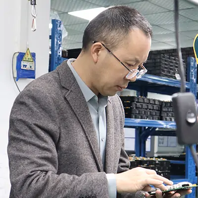
Manual Visual Inspection (MVI)
This is the most basic PCB inspection method.
The operator observes the surface of the circuit board with the naked eye or a
PCB microscope. They look for visible problems such as poor solder joints,
misaligned components or broken traces. This method is low-cost and easy to
operate, making it suitable for small-volume production or prototype testing.
However, due to the reliance on manual judgment, errors are prone to occur, and
it is impossible to detect invisible internal defects.
Automated Optical Inspection (AOI)
AOI automatically scans the circuit
board through high-resolution cameras and specialized software and then
compares it with the reference image. It can detect common issues such as
missing components, misalignment, soldering issues or polarity errors. This
inspection is an indispensable part of PCB quality control, particularly
suitable for mass production, featuring high speed, high precision, and repeatability.
X-Ray Inspection
PCB X-ray inspection is used to check
the hidden solder joints inside the circuit board, especially suitable for
packages such as BGA, QFN, and LGA. It can detect structural problems such as
solder voids, cold joints, layer misalignment or internal delamination. For
complex multilayer PCBs or products that require extremely high reliability
(such as medical devices and avionics), 3D X-ray systems can be used in
combination to provide more accurate internal imaging.

In-Circuit Testing (ICT)
ICT is a method of detecting component
performance and circuit connectivity by using test probes to contact test
points on circuit boards. It can verify whether resistors, capacitors, and
diodes are normal and also detect short or open circuits. This method is
suitable for mass production but requires the use of a customized test
fixture as well as programming. Although the preparation time in the early
stage is long, the detection efficiency is high, and it is one of the most
widely used PCB quality control methods.
Functional Testing
Functional testing is the final step
carried out after the PCB assembly is completed. It powers up the board and simulates
real operating conditions to verify whether the entire circuit works as expected.
This kind of test does not focus on the quality of detailed soldering but
rather on whether the entire board is working properly. It is an important step
for judging whether the product is qualified.
Flying Probe Testing
The flying probe test uses automatically
moving probes to test each circuit connection, without a custom fixture. This approach is
suitable for prototypes, small-batch or frequently modified products,
especially for the R&D stage. Although its testing speed is not as fast as
that of ICT, it is highly flexible and cost-effective and can effectively
complete conduction and insulation tests.
Hi-Pot Testing
Hi-Pot testing detects whether the
insulation performance is qualified by applying high voltage between different
circuits on the circuit board. It is mainly used to confirm that there will be
no leakage current or breakdown between circuits. This method is particularly
applicable to high-voltage products, such as power boards and EV controllers
and is an indispensable way of circuit board inspection in high-reliability
industries.
|
Inspection
Method
|
Main
Equipment
|
Inspection
Focus
|
Suitable
Scenarios
|
Advantages
|
Disadvantages
|
|
Manual Visual Inspection (MVI)
|
Naked eye, PCB microscope
|
Visible defects: bad solder joints,
misaligned components, broken traces
|
Small-batch production, prototype
testing
|
Easy to operate, low cost
|
Prone to human error, can’t detect
internal defects
|
|
Automated Optical Inspection (AOI)
|
High-res cameras, image processing
software
|
Missing components, misalignment,
solder defects, and polarity issues
|
Mass production, automated SMT lines
|
Fast, accurate, repeatable, scalable
for volume
|
Can’t detect internal layer or
under-component defects
|
|
X-Ray Inspection
|
X-ray scanner, 3D X-ray system
|
Hidden solder joints, voids, cold
joints, layer misalignment, internal delamination
|
Complex multilayer boards,
high-reliability products (medical, aerospace)
|
Reveals internal structure,
essential for BGAs and dense packages
|
High cost, complex operation
|
|
In-Circuit Testing (ICT)
|
Test probes, bed-of-nails fixture,
programming system
|
Electrical values (resistance,
capacitance), component function, shorts/opens
|
High-volume, standardized production
|
High precision, automated, detects
many faults in one run
|
Long setup time, requires a custom
fixture
|
|
Functional Testing
|
Power supply, signal/load simulators
|
Overall board performance under real
conditions
|
Final verification, system-level
testing
|
Verifies actual use-case performance
|
Can't locate the exact fault
location
|
|
Flying Probe Testing
|
Automated flying probe tester
|
Continuity and insulation without
fixture
|
Prototypes, small-batch, frequent
changes
|
No fixture required, cost-effective,
flexible
|
Slower than ICT, not ideal for
high-volume production
|
|
Hi-Pot Testing
|
Hi-Pot tester, high-voltage source
|
Insulation resistance, leakage,
breakdown detection
|
High-voltage boards (e.g. power
supply, EV)
|
Critical for safety, ensures
insulation between circuits
|
Not suitable for low-voltage
applications, safety precautions needed
|
By combining the use of the above
methods, manufacturers can control the quality of circuit boards at multiple
stages, achieve systematic PCB quality control, effectively improve the overall
PCB quality, reduce defect rates, minimize rework and after-sales issues, and
ensure stable product delivery.
Standards and Metrics in PCB
Inspection
When conducting PCB inspection, it is
necessary to determine whether the circuit board is qualified in accordance
with the industry-recognized standards. The two most commonly used standards
are IPC-A-600 and IPC-A-610, corresponding respectively to the requirements of
printed circuit board inspection at different stages.

1. IPC-A-600 (Bare Board
Acceptance)
IPC-A-600 is the standard used to
inspect bare boards. It mainly focuses on the physical characteristics of the
PCB, such as whether the overall dimensions meet the design requirements,
whether the hole sizes are accurate, whether the spacing between traces is
sufficient, and whether the safety distances are compliant. This standard is
commonly applied during the early stage of printed circuit board inspection
before components are mounted. By following this standard, manufacturers can
eliminate structurally non-compliant PCBs early in the production process and
avoid waste in later stages.
2. IPC-A-610 (Assembled PCB
Acceptance)
IPC-A-610 is the standard applied
after component mounting. It is used to determine whether solder joints are
full and reliable, whether the components are oriented correctly, and whether
there are any issues such as cold solder joints, solder bridging, or
misalignment. This standard is a very important part of later-stage PCB quality
control to ensure that assembled circuit boards meet functional and safety
requirements. It is especially indispensable in industries like medical and
automotive, where high reliability is critical.
Here is a comparison table of
IPC-A-600 and IPC-A-610 standards used in the circuit board inspection (circuit
board inspection) process:
|
Item
|
IPC-A-600
|
IPC-A-610
|
|
Applicable
Stage
|
Before
component mounting (bare board stage)
|
After
component mounting (assembly stage)
|
|
Inspection
Focus
|
Physical
characteristics: dimensions, tolerances, hole sizes, trace spacing, safety
distances
|
Solder
joint quality, component orientation, solder integrity, cold joints,
bridging, misalignment
|
|
Main
Purpose
|
Detect
bare board defects early to prevent issues in later assembly processes
|
Ensure
assembly quality and that the board meets functional and safety requirements
|
|
Role
in PCB Inspection
|
Used
during early-stage printed circuit board inspection (printed circuit board
inspection)
|
Core
part of late-stage PCB quality control (PCB quality control)
|
|
Applicable
Industries
|
All
industries involved in PCB manufacturing
|
Especially
important for high-reliability industries like medical, automotive, and
aerospace
|
|
Standard
Objective
|
Ensure
the structure of the bare board meets design and process requirements
|
Ensure
assembled PCBs function properly and meet delivery standards
|
These two standards are important
documents that must be referred to during the circuit board inspection process.
They can help manufacturers accurately judge the quality level of circuit
boards at different stages, thereby ensuring the reliability and consistency of
products in different application scenarios.
 About PCBasic
Time is money in your projects – and PCBasic gets it. PCBasic is a PCB assembly company that delivers fast, flawless results every time. Our comprehensive PCB assembly services include expert engineering support at every step, ensuring top quality in every board. As a leading PCB assembly manufacturer, we provide a one-stop solution that streamlines your supply chain. Partner with our advanced PCB prototype factory for quick turnarounds and superior results you can trust.
Common Defects Found During Inspection
During PCB manufacturing, whether
manual or automated inspection methods are adopted, some typical defect
problems are often encountered:
•
Solder Bridges:
When too much solder is applied, it connects two adjacent pads that should be
separate, forming a solder bridge. This short circuit can cause the circuit to
malfunction and may even damage components.
•
Voids:
These are gaps or bubbles inside the solder joints. They weaken the strength of
the joint and can affect electrical connectivity, potentially leading to poor
contact over time.
•
Component Misalignment:
When components are not placed accurately or are oriented incorrectly, it can
lead to functional issues or prevent the circuit from operating.
•
Lifted Pads:
Pads may detach from the PCB substrate due to excessive heat or external force.
This makes it difficult for components to be securely soldered, which affects
the durability of the product.
•
Insufficient Solder:
If there is not enough solder, the connection between the component and the pad
is weak. These weak joints may result in intermittent failures, especially in
environments with vibration or heat.
•
Cracked Traces:
Routing lines can break or burn out during processing or use. This causes the
circuit to lose connectivity and may cause certain functions to stop working.
These problems can all be detected
through appropriate circuit board inspection methods. Commonly used inspection
tools include automatic optical inspection (AOI), PCB microscope, and PCB X-ray
systems, which can help detect detailed problems that are invisible to the
naked eye, thereby improving the overall quality of PCBs.

Conclusion
In modern electronic manufacturing,
PCB inspection is very crucial. It can not only detect defects at an early
stage, but also help products comply with industry standards and enhance
customer satisfaction. Reliable PCB quality control is the foundation for
ensuring the long-term stability and reliability of products.
Whether using manual inspection, AOl,
PCB X-ray or functional testing, these methods are all helping us confirm
whether the circuit board is safe, stable and has good performance. With the
continuous advancement of technology, PCB quality control methods are also
becoming more advanced. Artificial intelligence and machine learning are
enhancing the speed and accuracy of inspections.
In today's world, where connectivity
and precision are essential, PCB inspection is not just a production step-it
represents manufacturing quality and professional standards.