Global high-mix volume high-speed PCBA manufacturer
9:00 -18:00, Mon. - Fri. (GMT+8)
9:00 -12:00, Sat. (GMT+8)
(Except Chinese public holidays)
Global high-mix volume high-speed PCBA manufacturer
9:00 -18:00, Mon. - Fri. (GMT+8)
9:00 -12:00, Sat. (GMT+8)
(Except Chinese public holidays)
HomePage > Blog > Knowledge Base > What is VCC? What is the Difference Between VCC and VDD?
The power pin names, such as VCC, VDD, VSS, and VEE, which look similar but are not the same, often leave people confused. They contain the core information of the circuit's working mechanism and are related to whether the power supply design of the entire circuit is correct. Especially VCC and VDD, they both represent the positive power pin of the chip, which often causes confusion. In different technical backgrounds and device types, there are differences in the usage, naming sources and applicable scenarios of these two terms. If their meaning is not clearly understood, it will not only easily lead to wiring errors, but also may cause serious consequences such as chip damage, power failure or abnormal signals.
To help readers understand the true meanings and usage norms of these two more clearly, we will conduct an analysis from several aspects, such as their meanings and functions, respectively, in this article. First of all, let's get to know the relevant content about VCC.
VCC is a very common term in electronic circuits. It is usually used to represent the positive power supply voltage in a circuit, especially in systems that use bipolar junction transistors (BJT) or TTL (Transistor-transistor Logic) circuits. To accurately understand circuit diagrams, datasheets and PCB designs, it is necessary to know the meaning and origin of VCC.

VCC is the abbreviation of "Voltage at the Collector". The letter "C" here is derived from the Collector of BJT. In early digital logic circuits, especially in TTL (Transistor-Transistor Logic), VCC represented the positive voltage supply provided to the collector side. To avoid confusion with VC, which represents "collector voltage", engineers have adopted a double "C" notation - VCC, which indicates the supply voltage rather than the node voltage.
In traditional transistor circuits, the collector is usually connected to the highest voltage point in the circuit - that is, the positive power rail. Therefore, VCC is used to represent a positive voltage line that supplies power to transistors and other components in a circuit. Although modern electronic products make greater use of field-effect transistors (FETs) and CMOS logic, the term VCC is still widely used due to historical conventions and the continuation of naming.
In electronic circuits, VCC typically represents the positive power supply line, providing working voltage for active devices such as transistors, microcontrollers, logic gates, and sensors. It is one of the most crucial power nodes in any electronic system. The following is a schematic diagram of VCC in a circuit:
In most digital or analog circuits, VCC stands for the main power rail, which provides energy inside the circuit. All active devices (such as integrated circuits) rely on a stable voltage source to operate normally, and VCC is the interface through which this voltage enters the device. For instance, in a single-chip microcomputer development board, VCC supplies power to the core logic.
In actual electronic circuits, VCC usually appears in the following forms:
The upward power rail symbol in the circuit diagram is marked as VCC
In the pin diagram of an IC, VCC is one of the power supply input pins
On the PCB board, "VCC" is usually silk-screened and marked beside the pins.
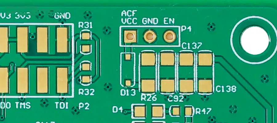
It appears as a named network in circuit design software such as KiCad and Eagle.
When the system has multiple voltage rails, you will also see similar names such as VCC1, VCC2, and VCC_IO, which are used to distinguish the voltage supply of different modules.
In actual design, VCC is not merely a name; it also has some distinct engineering characteristics:
1. The most common voltage values of VCC are 3.3V and 5V. 1.8V is also used in low-power systems, and 12V or 24V may be employed in industrial scenarios.
2. A continuous, stable and low-noise voltage must be provided for VCC; otherwise, it may lead to logical errors, restarts, and even chip burnout.
3. Decoupling capacitors should be added near VCC pins, and the power rail should be as short and thick as possible. Only in this way can voltage fluctuations be avoided.
VDD is also one of the most common power supply markings in electronic circuits. It usually represents the positive power supply voltage of devices that use MOSFET or CMOS logic circuits. Understanding what VDD is and how it differs from other power labels such as VCC is of great significance for reading circuit diagrams, datasheets and conducting PCB design.
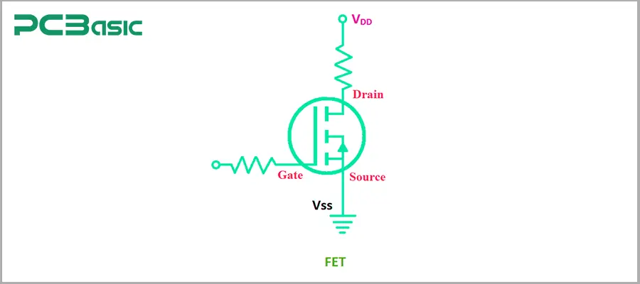
VDD is the abbreviation of "Voltage at the Drain", where the "D" comes from the “Drain” pin in the MOSFET. In modern electronic design, especially in digital logic circuits based on CMOS or NMOS processes, VDD is widely used as the standard term to represent the positive power rail.
In the MOSFET device structure, there are three main pins in total:
Gate: Receives control signals, functions as a switch, and basically does not consume direct current.
Drain: The terminal where current enters the device (from VDD).
Source: The input terminal of the current, usually grounded (i.e., VSS or GND).
When the MOSFET is on, the current path is usually VDD → Drain → Source → VSS (GND). As shown in the following figure:
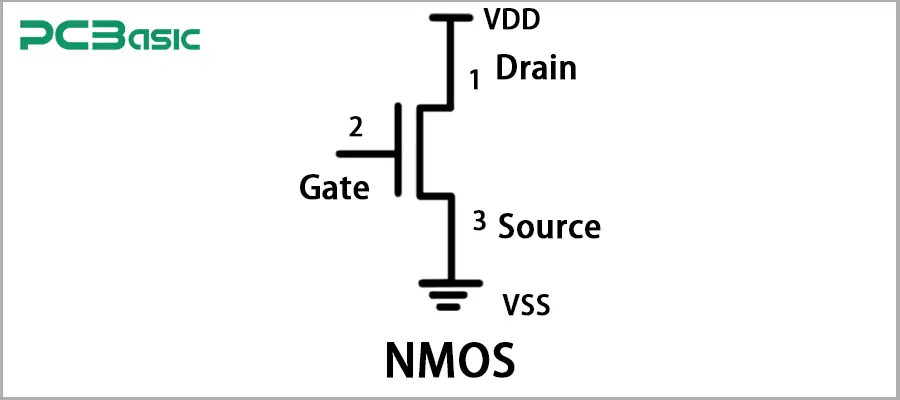
Since the positive power supply voltage is directly applied to the drain terminal, engineers named this supply voltage VDD. This naming has been in use to this day and is one of the common power tags in MOSFET architecture systems.
In the field of electronics, VDD usually refers to the positive supply voltage connected to the drain terminal of a MOSFET transistor.
VDD voltage is the main power supply rail in electronic systems, providing energy for the internal logic parts of digital devices. In CMOS logic circuits, VDD provides the core voltage required for the operation of devices such as microcontrollers, integrated circuits (ICs), memory chips, and system-on-chip (SoC).
Common VDD voltage values include:
1.8V - Low-power embedded system
3.3V - Microcontrollers and sensors are widely used
5V - common in old systems or mixed-signal designs
In circuit diagrams or PCB layouts, VDD is typically used to mark the positive power input pins of an IC. It defines the sources of operating voltage for logic gates and active devices.
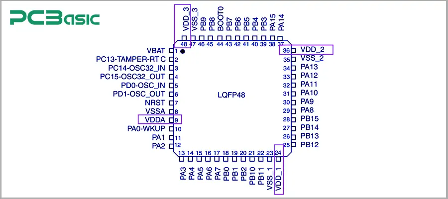
You may also see the following related signs:
VDD_IO - Power supply voltage for the IO interface
VDD_CORE - Core logic supply voltage
VDDA - Supply Voltage for Analog Circuits
In a MOSFET circuit, when the device is on, the current usually forms a path from VDD (drain) → Source (source) → VSS (ground). After having a certain understanding of VCC and VDD, let's take a look at the differences between the two.
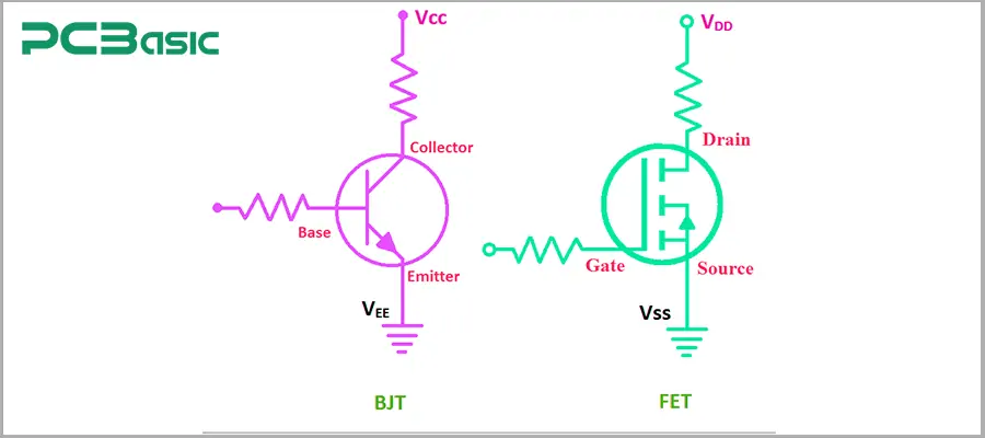
Both VCC and VDD are common positive supply voltage identifiers in electronic circuits, but they come from different transistor structures and are used in different types of circuits. Understanding the differences between the two is helpful for designing, reading and analyzing circuit diagrams more accurately.
VCC: Originating from BJT technology, it refers to "collector voltage"
VDD: Derived from FET technology, it refers to "drain voltage"
The two have different origins, but as technology has evolved, their practical applications in modern circuits have become similar.
Although they have different names, in actual circuits, VCC and VDD usually represent the positive power supply voltage. Different manufacturers use different terms based on the internal structure of the chips or naming conventions.
For example:
TTL chip → Use VCC
CMOS chip → Use VDD
|
Item |
VCC |
VDD |
|
Full Name |
Voltage at the Collector |
Voltage at the Drain |
|
Origin |
Comes from BJT (Bipolar Junction Transistor) circuits |
Comes from MOSFET (Metal-Oxide-Semiconductor) circuits |
|
Circuit Type |
Mainly used in BJT circuits |
Mainly used in CMOS or NMOS circuits |
|
Function Meaning |
Positive voltage supplied to the transistor's collector, usually the main power rail |
Positive voltage supplied to the transistor's drain, also the main power rail of a CMOS chip |
|
Associated Pin |
Collector |
Drain |
|
Typical Voltage |
Usually +5V or +3.3V |
Usually +5V or +3.3V |
|
Ground Reference |
VEE (Emitter voltage, often negative or ground) |
VSS (Source voltage, typically ground) |
|
Modern Usage |
Still used in analog or BJT-based circuits |
Commonly used in digital circuits, microcontrollers, and ICs |
Can VCC and VDD be used interchangeably?
In terms of circuit functions, VCC and VDD can be understood interchangeably. However, in actual design, one should always refer to the chip's data sheet to ensure correct wiring and avoid confusing the power logic.
For designers, the most important thing is to clearly mark their power lines, especially in hybrid device systems. Do not mix VCC and VDD on the same PCB to avoid confusion during maintenance and debugging.
Arduino:VCC vs VIN vs 5V
VCC: The voltage directly supplying power to the chip (usually 5V)
VIN: Input voltage terminal, usually connected to 9V or 12V
5V: The 5V power supply port output by the on-board voltage regulator
STM32 or ESP32: VDD, VDDA, VSS
VDD: Main Digital Power Supply
VDDA: Analog Power Supply
VSS: Ground Wire (GND)
Logic chips (such as the 74HC series)
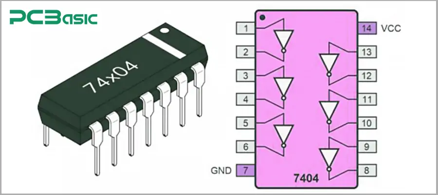
Use VCC as the positive power supply and GND as the ground wire
It is usually powered by 5V or 3.3V
How can VCC and VDD be used in actual circuits? First of all, of course, we need to identify VCC and VDD.
Before actual connection or testing, VCC and VDD on the circuit board must be correctly identified first. We can identify it in the following ways:
1. Check the PCB silk-screen label. Most PCBs will be marked with words such as VCC, VDD, GND, VSS or 3V3/5V on the pin header, power chip or beside the chip. As shown in the following figure
2. Consult the schematic diagram. In the schematic diagram, VCC and VDD are usually also marked on the power lines connected to the power supply pins of the chip.
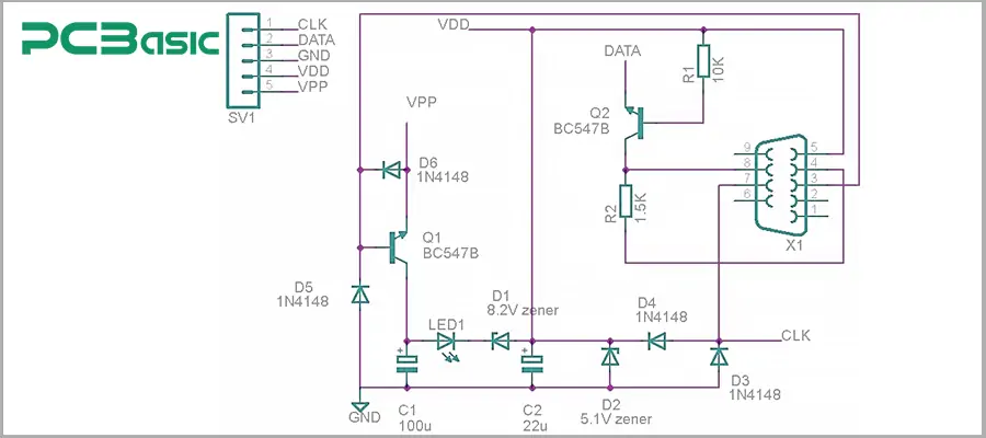
3. Refer to the device pin table. The datasheets of microcontrollers, sensors and other chips will clearly list which pin is VDD (power) and which pin is VSS (ground).
Correctly identifying VCC and VDD can prevent circuit damage caused by reverse power connection.
After identification, the voltage values of VCC and VDD can be measured with a multimeter to confirm whether the circuit power supply is normal.
First, set the multimeter to the DC voltage range: it is usually marked as "V⎓". Then, measure the voltage between VCC/VDD and GND/VSS: touch the red probe to VCC/VDD point and ground the black probe. Check if the voltage value is normal: for example, a 5V system should measure approximately +5.00V, and a 3.3V system should measure +3.3V. Check again if the polarity is correct: If it shows a negative value, it might be that the probe is connected in reverse or there is a wiring error in the circuit.
We should regularly check the power supply voltage, which is helpful to ensure the stability and reliability of the power supply voltage.
1. Use a voltage regulator to steadily convert the input voltage to the target VCC/VDD voltage.
Linear regulators such as AMS1117, 7805;
Switching regulators such as buck converters;
2. Add a Decoupling Capacitor to suppress noise and voltage fluctuations and ensure the stable operation of the chip.
3. Optimize the power routing of the PCB
A good PCB power layout is crucial for ensuring the stability of VCC/VDD, especially in high-frequency, high-speed or analog/digital hybrid systems. Here are several key suggestions for optimizing power supply wiring:
Reduce long-distance single-line power supply. Avoid powering multiple devices through a thin wire from a remote end, which may affect the stability of the system.
Use copper wires or Power planes that are wide enough to ensure that the power rail has sufficient width to reduce resistance and voltage drop.
Separate the analog power supply from the digital power supply to avoid the noise generated by the switching of the digital power supply from interfering with the analog circuit. When necessary, magnetic beads, inductors or low-noise LDOs can be used for isolation treatment.
4. Use power filter components
In actual circuit design, using appropriate power supply filter components is an important means to ensure that VDD power supply is "clean" and stable.
For circuits such as analog signal channels, RF modules or sensors, Ferrite beads or small inductors can be connected in series at their power input terminals to suppress high-frequency noise.
For analog devices such as analog-to-digital converters (ADCs) and digital-to-analog converters (DACs) that are extremely sensitive to power quality, it is recommended to use independent power rails in conjunction with filter devices. In this way, its VDD power supply is isolated from the main power system, which can ensure stable signals and reliable systems.
Through the above-mentioned design methods, we can significantly reduce power supply noise and enhance the anti-interference ability and precision performance of the circuit.
VCC and VDD are extremely important power supply identifiers. They are all terms used to refer to the positive power supply pins in electronic devices. In most cases, they have the same function in modern circuit design. Understanding their definitions, differences and identification methods on PCBs is a fundamental skill that every electronic engineer and developer must possess.
We should keep in mind:
VCC comes from the term "bipolar transistor" (BJT)
VDD comes from the term field-effect transistor (FET)
They can all represent the positive power supply pins of the chip
In the design, the data sheet should always be referred to to avoid incorrect connections
A good power supply layout not only ensures the normal operation of the circuit but also enhances the overall performance and reliability. Whether it's prototype design or mass production, handling VCC/VDD properly is a crucial step for you towards professional electronic design.
 About PCBasic
Time is money in your projects – and PCBasic gets it. PCBasic is a PCB assembly company that delivers fast, flawless results every time. Our comprehensive PCB assembly services include expert engineering support at every step, ensuring top quality in every board. As a leading PCB assembly manufacturer, we provide a one-stop solution that streamlines your supply chain. Partner with our advanced PCB prototype factory for quick turnarounds and superior results you can trust.

Assembly Enquiry
Instant Quote
Phone contact

+86-755-27218592
In addition, we've prepared a Help Center. We recommend checking it before reaching out, as your question and its answer may already be clearly explained there.
Wechat Support

In addition, we've prepared a Help Center. We recommend checking it before reaching out, as your question and its answer may already be clearly explained there.
WhatsApp Support

In addition, we've prepared a Help Center. We recommend checking it before reaching out, as your question and its answer may already be clearly explained there.