Global high-mix volume high-speed PCBA manufacturer
9:00 -18:00, Mon. - Fri. (GMT+8)
9:00 -12:00, Sat. (GMT+8)
(Except Chinese public holidays)
Global high-mix volume high-speed PCBA manufacturer
9:00 -18:00, Mon. - Fri. (GMT+8)
9:00 -12:00, Sat. (GMT+8)
(Except Chinese public holidays)
HomePage > Blog > Knowledge Base > PCB Manufacturing Process - A Comprehensive Guide
From the consumer electronics we come into contact with daily to the advanced aerospace systems, the core of these electronic devices is PCBs. Understanding the PCB manufacturing process is crucial for engineers, designers and enterprises that hope to obtain high-performance electronic products. The printed circuit board manufacturing process is not only related to performance and reliability, but also directly affects the delivery cycle and cost efficiency of the product. Mastering how to make a PCB is not only a part of technical learning but also the entry point for an in-depth understanding of what PCB manufacturing is.
Next, we will conduct an in-depth analysis of the PCB manufacturing process and systematically sort out the entire PCB manufacturing process. It is hoped that after you finish reading this article, it can help you fully understand the key steps and technical requirements of various PCB fabrication processes.
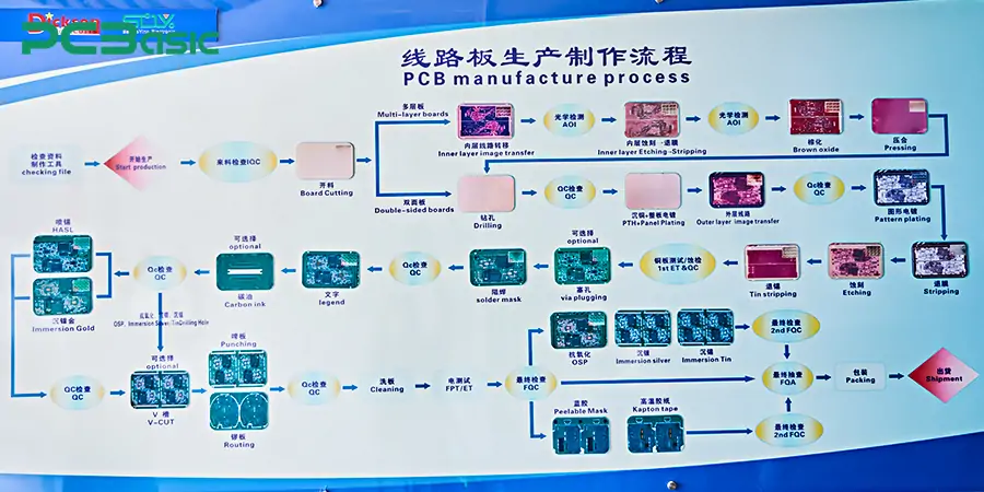
First of all, let's have a general understanding of PCB manufacturing. What is PCB manufacturing? In fact, PCB manufacturing is a multi-step process of converting design data into functional circuit boards. These processes include multiple key steps such as inner layer imaging, drilling, electroplating, etching, and surface treatment. Whether it is rigid boards, flexible circuit boards, rigid-flexible combination boards, HDI high-density interconnect PCBs, or ceramic PCBs, the manufacturing precision will directly affect the reliability of the final product. OK, now, let's learn how PCBs are made.
We will introduce it to you in 20 steps.
The first step in the PCB manufacturing process is to conduct a detailed review of all design and production documents. The content of the review generally includes the verification of Gerber documents and BOM (Bill of Materials), manufacturability design (DFM) analysis, as well as process planning and material preparation.
First, review the Gerber and BOM files. Review these documents to confirm the completeness and availability of the design data, to ensure that all key layers, holes, pads, solder masks and other design information of the circuit board are correct and error-free. This is the prerequisite for achieving high-quality PCB board manufacturing.
Then comes the analysis and evaluation of DFM. Analyze and evaluate whether the submitted design is suitable for the actual manufacturing capacity, regardless of the production scale. A good DFM can effectively reduce the production defect rate, increase the yield rate, and shorten the overall delivery cycle.
Then, there is the aspect of material preparation. PCB manufacturers need to select appropriate base materials, copper foil thickness, drilling methods, etc., based on the type of PCB (such as flexible boards, rigid-flex boards, or industrial-grade PCBs). In addition, detailed process flows will also be formulated during the pre-production stage, such as lamination parameters, electroplating plans and surface treatment technologies, to ensure that the entire PCB fabrication process is based on solid evidence.
Through these standardized pre-production review processes, circuit board manufacturing can make full preparations for subsequent production.
Inner layer imaging is a key step in transferring the circuit pattern from the design file to the surface of the copper foil. This step is generally involved in the production of types such as multilayer PCBs, HDI PCBs and rigid flex PCBs.
First, photosensitive adhesive was applied to the copper-clad substrate. Then, using laser direct drawing (LDI) or ultraviolet exposure, the circuit pattern will be precisely transferred onto the board surface. This step has extremely high requirements for the resolution and stability of PCB manufacturing equipment, especially in the manufacturing processes of flex PCBs and ceramic PCBs, where precise control is even more necessary. After the development process, the retained graphics will enter the etching process. This step will have a direct impact on the circuit quality of the PCB and is an important link for each PCB manufacturer to ensure the accuracy of the finished product.
After the graphic is developed, it enters the inner layer etching stage. This stage is a key process for transforming the design into the actual route. It is to remove the excess copper layer not covered by photoresist through chemical etching, thereby forming a clear circuit pattern.
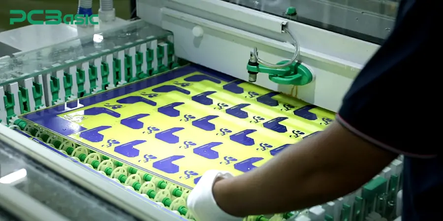
Chemical etching usually employs copper chloride or alkaline etching solutions and is completed under strictly controlled time, temperature and speed to ensure the integrity of the circuit and clear edges. After the etching is completed, the inner layer will be cleaned and dried, and then enter the lamination and alignment process to continue with the subsequent multilayer lamination process. Inner layer etching is a crucial step in ultimately transforming the design drawings into conductive solid circuits.
This process is not only applicable to prototype development but also widely used in the mass production stage, serving as a key bridge connecting design accuracy and electrical performance. And this process lays the foundation for high-quality PCB manufacturing and assembly.
After the inner layer etching is completed, the surface of the PCB is still covered with a layer of exposed photoresist. At this point, it is necessary to thoroughly remove this layer of residual photoresist through the peeling process to restore a clean copper surface. The cleaned copper surface must be free of residual glue and oxidation, as it serves as the basis for graphic electroplating and etching in the subsequent PCB manufacturing process. This step usually employs chemical or physical methods to remove the excess photoresist. Although this step is short, it is very important for the conductivity and interlayer bonding strength of the finished product.
After the inner layer graphics are completed, AOI technology needs to be used to detect whether there are any defects in the inner layer graphics of the PCB. AOI is a highly automated machine that can quickly detect defects in circuit design, such as short circuits, open circuits, and deviations, ensuring that each PCB board meets quality standards.
Immediately afterwards, in order to achieve the precise alignment of the multilayer boards in the subsequent lamination, the registration punching operation will be carried out. This step ensures strict layering alignment during the lamination process by drilling precise alignment holes in each layer. It is particularly suitable for the rigid flex PCB manufacturing process and the manufacturing of other high-layer boards. AOI inspection and positioning drilling are usually carried out in combination. On the one hand, this ensures the accuracy of the graphics; on the other hand, it guarantees the alignment of the structure.
In the multilayer PCB manufacturing process, oxidation treatment is usually carried out in order to enhance the bonding force between the inner layer and the prepreg (PP). Oxidation treatment is an optional step. This step is mainly used to enhance the bonding strength between the layers of multilayer PCBs and prevent delamination or voids during the lamination process. In the manufacturing process of multilayer PCBs, good interlayer bonding is crucial for ensuring the reliable transmission of electrical signals and the mechanical strength of PCBs.
Although not all products must undergo oxidation treatment, in high-end or industrial-grade PCB fabrication processes, it is an important guarantee for achieving high layer voltage quality.
Lamination refers to the process of stacking multiple inner copper foils and prepregs in a designed sequence and then pressing them together into a single unit under high temperature and high pressure conditions. This process enables the inner circuit boards to be firmly combined through insulating materials, forming a unified multilayer PCB structure.
The lamination process is widely used in various high-end PCB types, including HDI PCB, rigid flex PCB, and industrial PCB manufacturing process that requires heat resistance and high reliability. Lamination not only determines the electrical performance and structural strength, but also has a direct impact on the quality of subsequent steps such as drilling and electroplating. It is a key node for professional PCB manufacturers to demonstrate their process level.
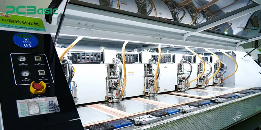
Drilling is mainly carried out by CNC drilling machines or laser drilling machines. The purpose of drilling is to provide precise holes for through holes and blind holes for establishing electrical connections between the board layers.
In the standard PCB manufacturing process, CNC drilling is widely used to produce through holes. In the HDI PCB manufacturing process, laser drilling technology is often adopted to process high-precision micro-blind holes and buried holes. The accuracy of drilling directly affects the subsequent conduction electroplating quality and is the basis for achieving multilayer interconnection in the entire PCB fabrication process.
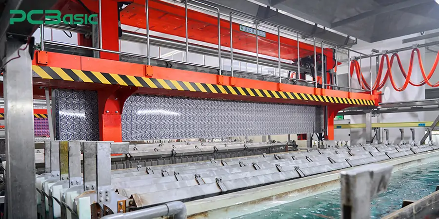
After the drilling is completed, the PCB enters the metallization and through-hole electroplating stage. This stage is a key step in achieving multilayer conduction connections.
Firstly, the residues on the pore walls need to be removed through chemical cleaning and activation treatment. Then, sensitization and catalysis are carried out on the non-conductive pore walls to prepare for the subsequent electroplating. Subsequently, electroless copper plating and electroplating copper techniques were adopted to uniformly deposit a layer of copper in each hole, forming a reliable conductive path.
This step is widely applied in the production of multilayer PCB, flex PCB and ceramic PCB. High-quality electroplated copper not only enhances the electrical conductivity of the sheet but also ensures the reliability of the connection.
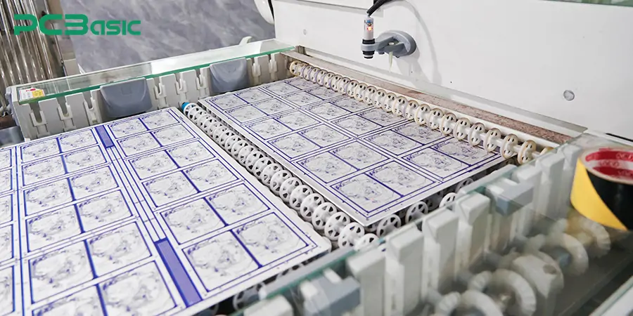
The transfer of outer layer graphics is one of the key steps in PCB manufacturing. At this stage, the circuit pattern is coated with photoresist and exposed to form the initial structure of the circuit.
First, apply a layer of photoresist on the outer copper surface, and then expose it through laser direct tracing (LDI) or ultraviolet exposure technology. The exposed resist will form an anti-corrosion layer on the circuit board to protect the areas that do not need to be etched. This process needs to be carried out under strict lighting conditions to ensure the clarity and accuracy of the circuit and precisely transfer the circuit pattern onto the resist.
After exposure and development, only the area covered by the circuit pattern will be retained on the board surface. The accuracy of the outer layer pattern is directly related to the quality of the final pad and the solderability of the component, and it is a key link to ensure functional reliability in the PCB fabrication process.
After the transfer of the outer layer graphics is completed and developed, the PCB manufacturing process enters the stage of copper thickening and tin protection. This step involves electroplating in the circuit pattern area to thicken the copper layer and enhance electrical conductivity and mechanical strength. The purpose of the copper coating is to further thicken the exposed copper surface to enhance the conductivity and corrosion resistance of the circuit.
Subsequently, a layer of tin protective layer is electroplated on the thickened copper surface. The tin plating layer is to protect the copper layer from the influence of the subsequent etching process, preventing the copper layer from oxidizing or being corroded. The tin layer only covers the circuit area. The non-circuit area not covered by the photoresist will be removed in the next etching.
The coating quality of copper and tin is directly related to the electrical performance and graphic integrity of the finished board, and it is an indispensable step in the PCB fabrication process.
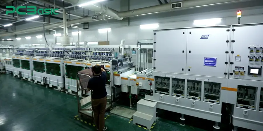
After the copper thickening and tin protection are completed, the PCB manufacturing process enters the stage of stripping the outer layer of resist. Stripping usually employs chemical solutions to thoroughly remove photoresist without damaging the copper surface and tin layer, preparing for the next etching process. The purpose of this step is to remove the residual photoresist on the outer layer and only retain the circuit area that has been tin-plated for protection. After completing this step, the graphics on the circuit board can start to be etched, removing the unprotected copper layer, and finally forming a fine circuit pattern.
Although this step is brief, it is crucial for ensuring the integrity of the line and the quality of the outer graphic. It can reflect the PCB manufacturer's strict control over details and stability.
After the outer layer of the resist is stripped off, the PCB manufacturing process enters the final etching stage. The final etching process is a crucial step in PCB manufacturing to remove unprotected excess copper layers, which helps form the final circuit pattern of the circuit board. This process usually requires the use of chemical etching solutions (such as ferric chloride or hydrofluoric acid) to remove the exposed copper layer. After the etching is completed, the protective tin layer is peeled off to make the final circuit pattern fully visible. This process is widely applied in the manufacturing processes of multilayer PCBs, HDI PCBs and rigid flex PCBs. These types of circuit boards have extremely high requirements for etching accuracy and graphic edge quality.
The final etching is the last step in the formation of the circuit. This process directly determines the clarity and conduction performance of the circuit.
After the circuit diagram is completed, it comes to the stage of coating the solder mask layer. This step involves applying a layer of green, black or other colored solder mask ink on the PCB surface, followed by hardening treatment through UV curing or thermal curing processes. Only Windows are reserved at the positions that need to be soldered, such as pads and vias.
The solder mask is used to protect copper circuits from short circuits or oxidation during the soldering process. High-quality solder mask layers not only enhance the durability and anti-pollution ability of PCB boards, but also form the basis for achieving high-density PCB manufacturing and assembly.
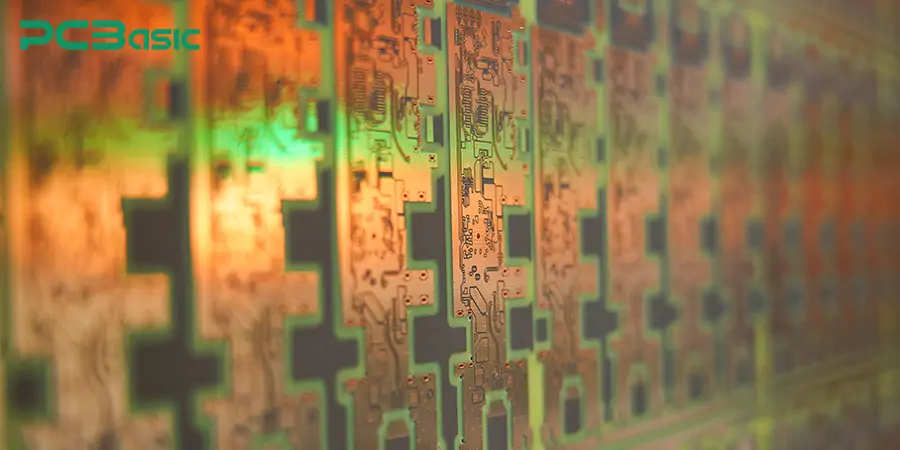
After the solder mask curing is completed, the PCB enters the surface treatment stage. PCB surface treatment is a key process in the PCB manufacturing process to ensure solderability and long-term reliability. Common surface treatment processes include: ENIG, HASL, OSP, silver plating/gold plating. The main function of these treatment methods is to enhance the solderability of the pad surface and prevent the oxidation of the copper layer.
The choice of surface treatment will affect the soldering quality, storage life and electrical performance of components, and it is an indispensable part of the high-quality PCB manufacturing process.
Screen printing is a process used to print necessary markings on the surface of PCBs, such as component numbers, logos, assembly markings, etc. In some industrial PCB manufacturing processes, screen printing not only involves assembly markings but may also include information such as barcodes or QR codes, which facilitate tracking and quality control.
The silkscreen layer is usually printed with special inks, which can ensure that the logo is clear and long-lasting. The ink used is usually white or yellow and is printed on the surface of the solder mask layer without affecting the electrical performance. This step ensures the identification and functionality of the PCB during assembly and later use, and is a necessary step to improve the efficiency and readability of PCB manufacturing and assembly.
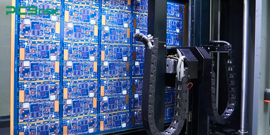
Electrical testing is the last key quality inspection process in the PCB manufacturing process, used to detect the conductivity and insulation of all circuits on the PCB to ensure there are no defects such as short circuits and open circuits.
One of the common methods is flying probe testing. Flying probe testing is carried out by using a high-speed moving probe to check one by one between test points. This type of test does not require the production of test fixtures and is particularly suitable for small-batch sampling or multi-variety production. It has the advantages of flexibility, high efficiency and low cost.
After passing the electrical test, the PCB enters the forming and cutting stage, which is the process of cutting large boards into single or assembled finished products. During this process, CNC equipment is usually used to perform high-precision shape cutting on the PCB to ensure that the dimensional tolerances meet the design requirements.
For products with a panel structure, V-scoring treatment is of vital importance. By performing V-scoring on the assembled panels, it is convenient to carry out subsequent panel separation operations and avoid damaging the single panels in the subsequent steps. This process is very common in PCB manufacturing and assembly and can significantly improve mounting efficiency and reduce the assembly cost.
In the final stage of the PCB manufacturing process, all finished products need to undergo strict final quality inspections to ensure that the electrical performance, mechanical structure and appearance quality fully comply with the specifications. The main items inspected include:
Appearance inspection (scratches, bubbles, contamination, etc.)
Automatic optical inspection (AOI) to confirm the integrity of the graphics
Dimensional measurement and hole position confirmation
The quality grade is evaluated in accordance with the IPC Class II/Class III standard
This inspection process ensures that the products meet the design and industry standard requirements before leaving the factory. It is the last line of defense to guarantee the consistency and reliability of PCB manufacturing and assembly.
After all the tests are completed, PCBs can be packed and shipped.
First of all, PCB manufacturers need to bake the PCBs to remove residual moisture and prevent moisture from affecting the soldering quality. Subsequently, vacuum packaging and anti-static packaging were adopted to effectively protect the copper layer on the board surface and the component pads, especially for environmentally sensitive products such as flex PCBs and HDI PCBs.
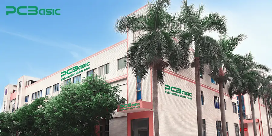
PCBasic is a leading PCB manufacturer. With its comprehensive certifications, strong manufacturing capabilities and outstanding delivery speed, it is the preferred partner of many customers. Below, we will elaborate on the advantages of PCBasic in the field of PCB manufacturing:
Whether you need thin, flexible and bendable circuit boards, industrial PCBs with high current carrying capacity, or medical-grade HDI boards with precise interconnection and high reliability, PCBasic can provide high-quality, traceable, and mass-producible PCB manufacturing and assembly solutions with its rich experience and advanced equipment.
From consumer electronics to critical aerospace systems, the PCB manufacturing process is crucial to modern electronic products. Mastering each key step helps engineers and purchasers make informed decisions. PCBasic is equipped with advanced PCB manufacturing facilities, an experienced engineering team and a complete quality control process. No matter how PCBs are manufactured or the specific operations in the PCB manufacturing process, PCBasic can provide customers with professional solutions to ensure that every step of the product from design to production is flawless.
After reading this article, you must have gained a deeper understanding of the PCB manufacturing process, right? And if you are evaluating how to make a PCB or looking for a reliable PCB manufacturer, PCBasic is undoubtedly your trustworthy partner.
 About PCBasic
Time is money in your projects – and PCBasic gets it. PCBasic is a PCB assembly company that delivers fast, flawless results every time. Our comprehensive PCB assembly services include expert engineering support at every step, ensuring top quality in every board. As a leading PCB assembly manufacturer, we provide a one-stop solution that streamlines your supply chain. Partner with our advanced PCB prototype factory for quick turnarounds and superior results you can trust.
Assembly Enquiry
Instant Quote
Phone contact

+86-755-27218592
In addition, we've prepared a Help Center. We recommend checking it before reaching out, as your question and its answer may already be clearly explained there.
Wechat Support

In addition, we've prepared a Help Center. We recommend checking it before reaching out, as your question and its answer may already be clearly explained there.
WhatsApp Support

In addition, we've prepared a Help Center. We recommend checking it before reaching out, as your question and its answer may already be clearly explained there.