Global high-mix volume high-speed PCBA manufacturer
9:00 -18:00, Mon. - Fri. (GMT+8)
9:00 -12:00, Sat. (GMT+8)
(Except Chinese public holidays)
Global high-mix volume high-speed PCBA manufacturer
9:00 -18:00, Mon. - Fri. (GMT+8)
9:00 -12:00, Sat. (GMT+8)
(Except Chinese public holidays)
HomePage > Blog > Knowledge Base > Key PCB Assembly Machines Behind Reliable PCBA Manufacturing
In this article, we will take you on a deep dive into the key PCB assembly machines used in modern manufacturing, including pick-and-place machines, soldering machines, and various inspection machines. Whether you are an OEM enterprise seeking reliable manufacturing partners or want to gain a comprehensive understanding of the core driving forces behind an efficient PCBA production line, this article will reveal the key PCB assembly machines that leading manufacturers in the industry rely on. OK, let's get straight to the point now!
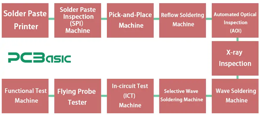
In the entire PCB assembly process, different types of professional equipment are required at different stages. From solder paste printing, component mounting, to soldering, inspection and testing, advanced automated equipment not only enhances production efficiency but also directly affects the yield and stability of the final PCBA products. Below, we will introduce the key PCB assembly machine to you based on the assembly process flow.
In the standard surface mount PCB assembly process, solder paste printer is the first core equipment of the entire production line. It is usually used after the PCB loading or cleaning process. Its main function is to precisely print a uniform layer of solder paste on the pads on the surface of the printed circuit board, laying the foundation for component mounting and subsequent soldering.
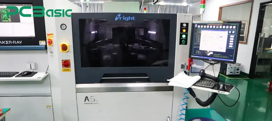
At this stage, the exposed PCB will automatically enter the solder paste printer through the conveying system. Then the device uses a high-precision visual positioning system to precisely align the PCB with the solder stencil. Then, the solder paste is evenly printed onto the pad position through the scraper system. The key control parameters of this process include the pressure and speed of the scraper, the viscosity of the solder paste, the thickness of the stencil, etc. Even a slight deviation may affect the subsequent placement quality.
This equipment is widely used in the SMT machine for PCB assembly production lines and is one of the key PCB assembly machines. After the solder paste printing is completed, the PCB will enter the next machine: SPI machine, namely the solder paste inspection machine.
The solder paste inspection machine is a key quality control link in the SMT production line. It is specifically designed to test the quality of solder paste printing and ensure the accuracy and consistency of printing. It will conduct high-precision three-dimensional detection of the solder paste printing results on the PCB surface and evaluate the following key parameters:
1. Is the position of the solder paste accurately placed on the pad?
2. Whether the volume, height and area of the solder paste comply with the process standards;
3. Whether there are defects such as insufficient solder paste printing, offset, solder bonding, missed printing or collapse.
Through these test data, problems such as printing deviations or stencil blockages can be detected early. This can effectively prevent defects from flowing into the SMT process and improve the yield rate.
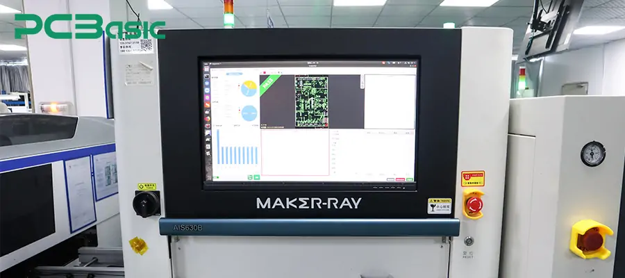
SPI machines typically employ laser or projection grating and camera imaging systems to rapidly scan the solder paste on each pad and generate 3D solder paste images. At this stage, the PCB board is fed into the SPI device through the conveying system. Then, the camera scans each pad to obtain the three-dimensional information of the solder paste. The system will automatically compare the solder paste image with the standard value set by the program. It then automatically determines whether there are defects and feeds back abnormal data to the operator or the MES system.
The SPI machine is one of the indispensable quality control devices in the entire SMT automated production process. It not only ensures the quality of solder paste printing, but also guarantees the quality of soldering and product reliability. After passing the SPI detection, the PCB will continue to be transmitted to the pick-and-place machine.
The pick-and-place machine is also one of the most core and crucial devices in the SMT production line. It is responsible for precisely mounting electronic components onto the designated pad positions on the surface of the PCB board. This includes:
1. Grab components from material tapes, trays or reels;
2. Align the device and PCB coordinates through the visual recognition and positioning system;
3. Mount the devices onto the solder paste printing area at an extremely high speed and with high precision.
It is a key link in the entire PCB assembly that affects speed and accuracy. Whether it is tiny 0402 resistors and capacitors or larger complex packaged devices such as ICs, BGA, and QFPs, it can achieve automated, batch, and error-free placement.
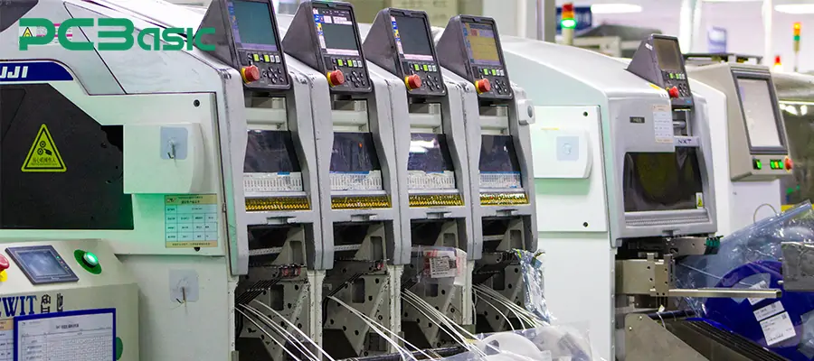
The pick-and-place machine sucks components through the vacuum suction force of the Nozzle system. The high-speed X-Y moving platform then quickly and accurately moves the suction nozzle to the designated coordinate. The visual recognition system identifies the orientation and angle of components and aligns them with the PCB. Then, through the control system and program library, the precise control of component coordinates, angles, and mounting sequence is achieved.
The entire process can be summarized in one sentence: "quick picking, precise mounting." After the high-speed mounting of the pick-and -place machine for PCB assembly is completed, the surface of the PCB is already covered with various precisely placed electronic components. Next comes the soldering process.
A reflow soldering machine is the key equipment for completing electrical connections throughout the surface mount PCB assembly. It achieves true electrical conduction by melting the solder paste through a controlled temperature curve and firmly bonding it with the pads and component pins.
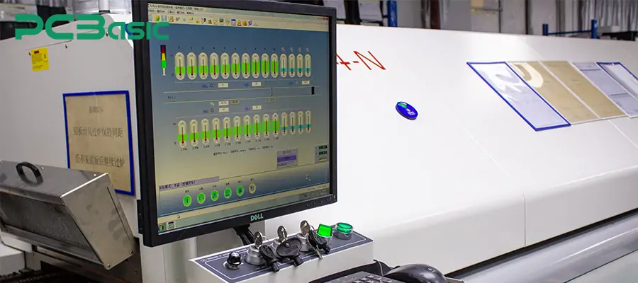
The main function of the reflow soldering machine is to heat the solder paste to its melting point within a precisely controlled temperature range. Thus, the assembled components are soldered onto the PCB board. This device can complete the transformation from physical contact to electrical connection between the PCB and components. During this process, the PCB will pass through the conveying system into multiple temperature zones (preheating zone, constant temperature zone, reflow zone and cooling zone), where the solder paste melts and solidifies, thus completing the soldering.
High-quality soldering relies on scientific reflow curve design, mainly including the following stages:
Preheating stage: Gradually increase the temperature to prevent thermal shock to the components.
Constant temperature stage: Ensure uniform temperature throughout the PCB.
Reflow stage: Reach the melting point of the solder paste (approximately 217℃ to 245℃), and complete the soldering.
Cooling stage: Rapidly cool down to form reliable solder joints.
An accurate temperature control system is the core criterion for measuring the performance of automatic PCB assembly machines such as reflow soldering.
After the PCB is soldered through the reflow oven, the components have been firmly connected to the circuit board. However, to ensure the quality of solder joints and the accuracy of mounting, meticulous visual inspection must be carried out. At this point, the PCB enters the crucial AOI equipment.
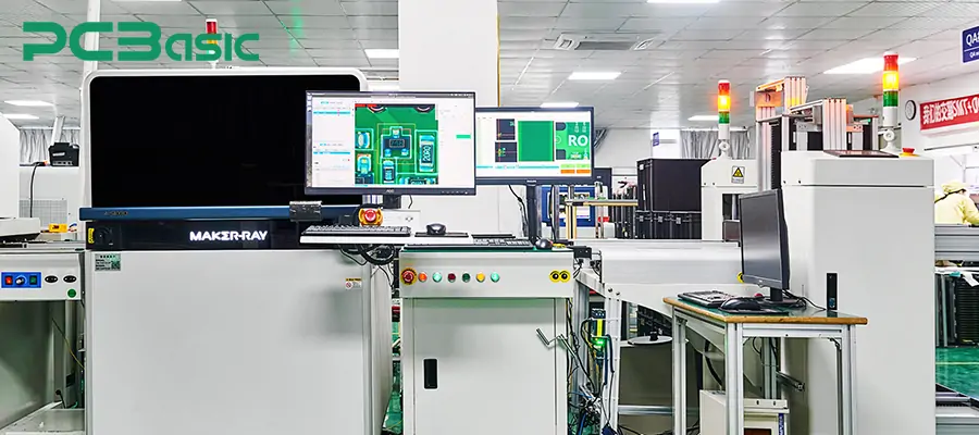
The AOI machine employs high-definition industrial cameras and image processing algorithms to conduct rapid and high-precision inspections of PCBs after soldering. Its core tasks include:
1. Check the integrity of the solder joints and soldering defects (such as false soldering, continuous soldering, insufficient solder, solder balls, etc.);
2. Detect component offset, reverse, missing parts or incorrect polarity;
3. Realize fully automatic quality control and defect marking for the entire board.
Through AOI, various defects generated in the pick-and -place machine for PCB assembly or reflow soldering can be effectively screened out. This has greatly enhanced the product yield and traceability. It can be deployed at various stages of SMT, such as after solder paste inspection, after surface mount technology (SMT) placement, and after reflow soldering, as part of multi-level quality control measures.
For package types such as BGA, QFN, and LGA where solder joints are hidden at the bottom of the device, ordinary optical equipment cannot image and identify them. At this point, a more advanced Inspection device - X-Ray Inspection Machine - is needed. X-Ray equipment belongs to the sophisticated automated PCB assembly machine. It is usually composed of several parts, including an X-ray source, a digital flat panel detector (FPD), an image processing system, and an automatic determination function. Some advanced models are also equipped with CT scanning functions, which can generate three-dimensional tomographic images of solder joints or solder balls.
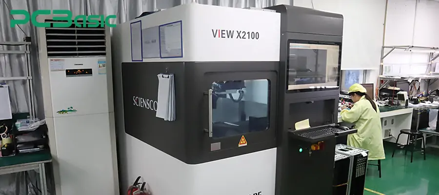
X-ray inspection equipment can detect the following defects without damaging components by conducting low-dose high-resolution X-ray scanning on PCBs:
1. Problems such as false soldering, voids, cold soldering, and bridging under BGA or QFN;
2. Interlayer connection defects within multi-layer boards;
3. Whether the distribution of the solder balls is uniform and whether the degree of collapse is qualified;
4. Internal structural issues of components (such as broken pins or displacement).
It is the only effective way to detect the quality of solder joints at the bottom of the package and hidden defects. It is a detection machine as crucial as AOI.
After the SMT reflow soldering process is completed, the PCB has finished soldering the surface mount components. And through the inspection by high-precision equipment such as AOI and X-Ray, the soldering quality and reliability are ensured. However, for those components that cannot be assembled using surface mount technology, such as transformers and large capacitors, THT technology must be adopted for assembly. At this point, a wave soldering machine is needed.
A wave soldering machine is a device specifically designed for automatic soldering of through-hole components, suitable for the mixed assembly process after SMT reflow soldering. The principle is to insert components into the through holes of the PCB, and use the peaks of the molten solder at high temperatures to come into contact with the pads and the pins of the components, completing rapid and uniform soldering.
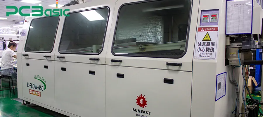
After the plug-in is completed, the PCB enters the equipment conveying system.
1. First, evenly heat up through the preheating zone to avoid thermal shock during soldering.
2. Then, the flux spraying system is applied beneath the PCB.
3. Then, after passing through the peak area of the molten solder, the solder surges to the bottom of the pin, forming a solder joint.
4. Finally, enter the cooling zone to rapidly solidify the solder points.
The key components of a wave soldering machine include the preheating system (hot air or infrared), flux spraying system, cooling system, conveying system, etc. The wave soldering machine is the main equipment for achieving through-hole soldering and also a key hub for the integration of SMT and THT processes in modern electronic manufacturing.
If the THT components are small, scattered, or adjacent to the area where SMT components have already been installed. At this point, if traditional full-board wave soldering is used, it is easy to cause thermal damage to the already mounted components or poor soldering. To address this demand for local soldering, selective wave soldering is required. It can utilize programmable nozzles or microwave peaks to precisely heat and solder only the target solder joints. This can avoid causing thermal effects on the surrounding areas.
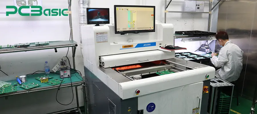
After the THT soldering process is completed, at this point, the post-solder AOI equipment will be used. This device is specifically designed for inspecting the appearance quality of through-hole solder joints, as well as issues such as incorrect insertion positions and polarity of components.
After a comprehensive inspection of the soldering quality through the AOI equipment, if there are no appearance defects such as false soldering, insufficient solder, or offset, the electrical testing stage can be entered.
The ICT test machine is an efficient and automated PCB assembly inspection machine, specifically designed to detect the electrical connection status of each component and circuit node on the PCB board. It detects each test point on the PCB one by one through the low-voltage power supply and signal source. It then compares the network meter file (Netlist) within the system with the actual measured values to achieve automatic determination. Its components include a needle bed test fixture (the fixture needs to be customized according to the PCB), a multi-channel power supply and electrical measurement module, a control platform and test program software, etc.
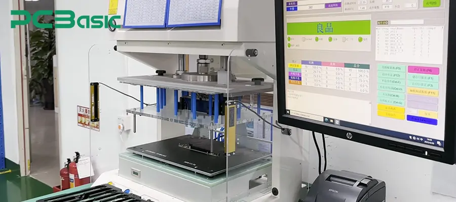
1. Check whether the components are placed correctly (polarity, direction, type);
2. Test whether the nominal values of resistors, capacitors, inductors, etc., are normal;
3. Check whether there are faults such as open circuit, short circuit and bridge connection in the welding.
4. Verify the connection of the power pins of the IC and the arrangement of bypass capacitors;
5. Determine whether the PCB netlist is consistent with the design.
Although ICT machine has the advantages of high efficiency and high precision in mass production, it requires custom-made dedicated needle bed fixtures, which result in high production costs and long delivery cycles. At this point, the flying probe tester, as a device that does not require fixtures and automatically executes the test path, is an ideal choice.
Flying probe tester is a high-precision and programmable PCB assembly inspection machine. It directly contacts the test points on the PCB board through a movable probe system to conduct electrical connection tests on each component and circuit after soldering. Unlike ICT, flying probe testing does not require a needle bed fixture, and thus is particularly suitable for the testing needs of small-batch, diverse or high-density products.
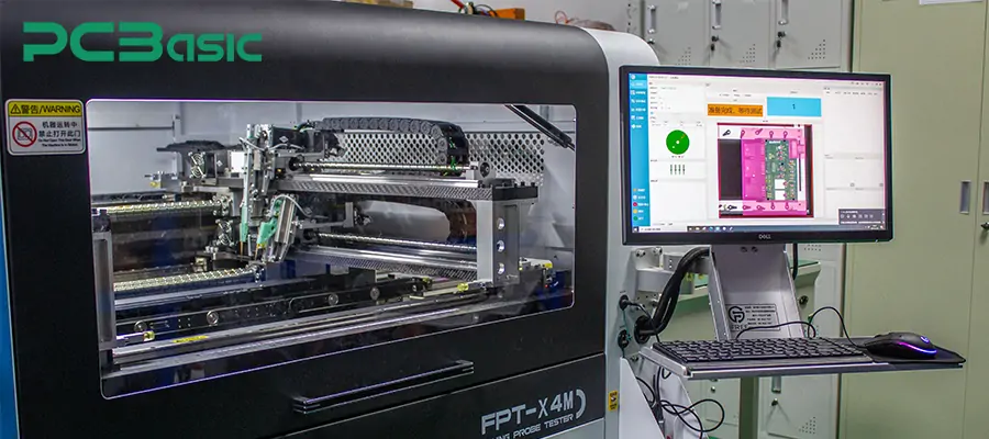
1. Detect the electrical values (resistance, capacitance, inductance, etc.) of components on the PCB;
2. Check for open circuits, short circuits, Bridges and missed welds.
3. Identify the polarity direction and the problem of components being inserted in reverse;
4. Verify whether the PCB network connection is consistent with the design;
5. Some high-end models support simultaneous testing and debugging, as well as learning paths while testing.
After passing the ICT or flying probe test, the circuit board meets the conditions for "power-on testing", and then functional testing equipment is needed.
FCT functional testing equipment is a testing system used to verify the actual operating effect of circuit boards. This equipment is usually carried out after the entire board has completed all SMT and THT processes and passed the electrical test. The FCT equipment will truly power on the circuit board and load the input signal, simulate the operating status of the terminal product, and detect whether the functions of each sub-module and interface are normal. This type of equipment is widely used in the finished product testing links of electronic control boards, power supplies, motor drives, communication modules, consumer electronic products, etc.
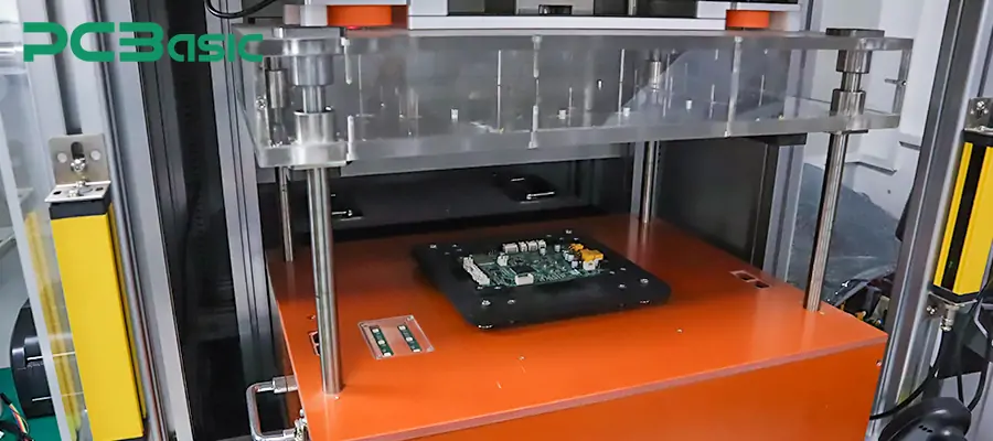
1. Can the PCB start power supply normally and check for overcurrent/undervoltage;
2. Whether the main control chip (such as MCU/SoC) can respond correctly;
3. Whether the communication interfaces (such as UART, USB, CAN, SPI, etc.) are unobstructed;
4. Whether the input and output of analog/digital signals conform to the set values;
5. Whether the functions of external drive, relay, buzzer, button, LED, etc. are normal;
6. Whether the actual load responses of motor control, screen display, sound playback, etc. meet the standards.
At this point, the entire PCB assembly production line has completed the full process from mounting, soldering, inspection to final performance verification. Functional testing ensures that each PCBA can meet the design requirements and customer standards in the actual operating state after being powered on. It is a crucial step to ensure product reliability and shipment quality.
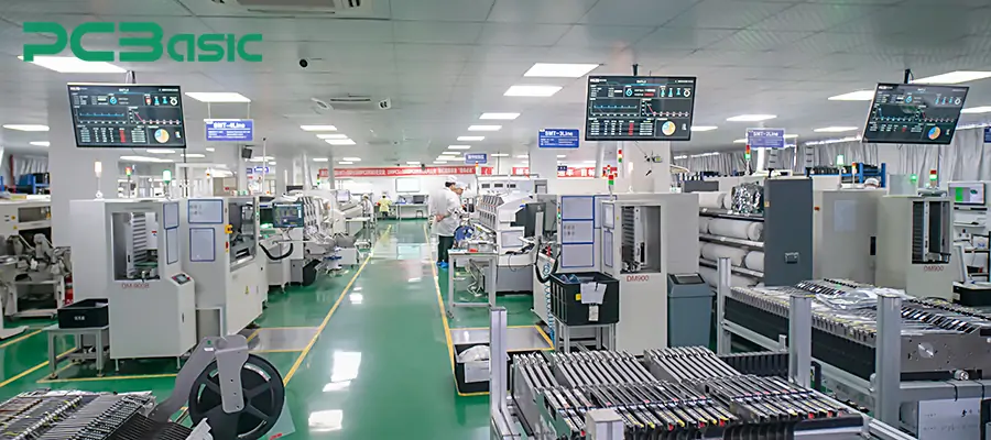
The reliability and performance of PCBA products largely depend on the precision and capacity of the production equipment adopted. PCBasic, a leading PCBA manufacturer in the industry, possesses a complete set of advanced PCB assembly production lines.
Our production workshop is equipped with advanced PCB assembly machines, including fully automatic solder paste printers, SPI equipment, pick-and-place machines, reflow soldering machines, AOI machines, wave soldering machines, selective soldering machines, ICT machines, flying probe testers, and functional testers (Learn more: IPC class 3 and PCBA test)
Our automated production line not only supports the hybrid process of SMT and THT, but also can flexibly meet the assembly requirements of various complex circuit boards. Choose PCBasic as your PCBA manufacturing partner and make quality, efficiency and precision the standard for every circuit board.
Time is money in your projects – and PCBasic gets it. PCBasic is a PCB assembly company that delivers fast, flawless results every time. Our comprehensive PCB assembly services include expert engineering support at every step, ensuring top quality in every board. As a leading PCB assembly manufacturer, we provide a one-stop solution that streamlines your supply chain. Partner with our advanced PCB prototype factory for quick turnarounds and superior results you can trust.
 About PCBasic

Assembly Enquiry
Instant Quote
Phone contact

+86-755-27218592
In addition, we've prepared a Help Center. We recommend checking it before reaching out, as your question and its answer may already be clearly explained there.
Wechat Support

In addition, we've prepared a Help Center. We recommend checking it before reaching out, as your question and its answer may already be clearly explained there.
WhatsApp Support

In addition, we've prepared a Help Center. We recommend checking it before reaching out, as your question and its answer may already be clearly explained there.