Global high-mix volume high-speed PCBA manufacturer
9:00 -18:00, Mon. - Fri. (GMT+8)
9:00 -12:00, Sat. (GMT+8)
(Except Chinese public holidays)
Global high-mix volume high-speed PCBA manufacturer
9:00 -18:00, Mon. - Fri. (GMT+8)
9:00 -12:00, Sat. (GMT+8)
(Except Chinese public holidays)
HomePage > Blog > Knowledge Base > PCB Manufacturing Process — A Step-by-Step Guide
The printed circuit board (PCB in short) is the result of a complex PCB manufacturing process that runs in hundreds of PCB board-making factories worldwide.
This article covers the PCB manufacturing process steps and what professional PCB manufacturing facilities prepare to fabricate the final product we see and use in our daily lives. From PCB design to PCB board manufacturing, we guide you step by step through the PCB design and manufacturing PCB process to make wiser decisions.
Every PCB starts from a hand-crafted PCB design by a professional PCB designer. A PCB design factory can provide custom design services. Usually, the customers will provide and upload their already made files ready for PCB production. Once this stage is done, The PCB manufacturing process is beginning.

Many professional PCB manufacturing facilities designed an online quotation system that enables the customer to get online order quotations almost instantly. If the customer requires specifications or demands regarding the PCB production process, the quotation form also allows the ability to leave a note. An online quotation is often a rough estimation. The price will be updated once a manual verification by the PCB facility is completed. PCBasic is an online PCB maker with a complete online quotation system.

The laser cutter/printer used in the PCB manufacturing facility is exact and accurate. Using the uploaded Gerber files, the PCB factory will produce something called a photo film. That photo film is similar to paper printed from a laser printer, although different in material and consistency due to its nature and use. The film outlines the PCB design, and each film will be made separately for each layer of PCB. For instance, for a 2-layer PCB, four films will be made, two used for the board layers and the other two designed for the solder mask.
It’s a well-known fact that PCB is made primarily out of copper. The previous step of laser cutting a film to create an outline is crucial for PCB production. The PCB manufacturing facility will use the system to shine UV light into the copper sheets. This will cause particular places over the sheets to harden, making the layout visible.
It’s imperative to keep a sterile environment during this process. That includes no exposure to dust or other types of unwanted particles. During the copper preparation stage, such unwanted particles can cause a short circuit or damage to the fabricated PCB
Once the fabrication is over, the copper boards are washed using an alkaline solution to ensure no leftover material is left unhardened.
This PCB board manufacturing stage is usually done for PCB designs with over two layers. A superficial two layers PCB board can be drilled without the UV technique.
The Electronics PCB manufacturing process includes the use of different types of chemicals. During the previous stage, an alkaline solution was used to ensure no material was left unhardened after the UV blasting process.
The PCB manufacturer soaks the boards in a copper solvent solution to ensure no unwanted particles are left on the fabricated copper boards. This solution, made of powerful chemicals, will provide no excess materials are left on the board.
Once this process is done, the copper board will be shiny and ready for the next PCB manufacturing steps.
At this stage of PCB board making, we should end up with separated copper sheets ready for inspection. The PCB manufacturer makes the process by aligning the sheets together and punching them in. This process is crucial because there is no way to correct any mistakes made in the inner layers of the PCB once the sheets are bonded together.
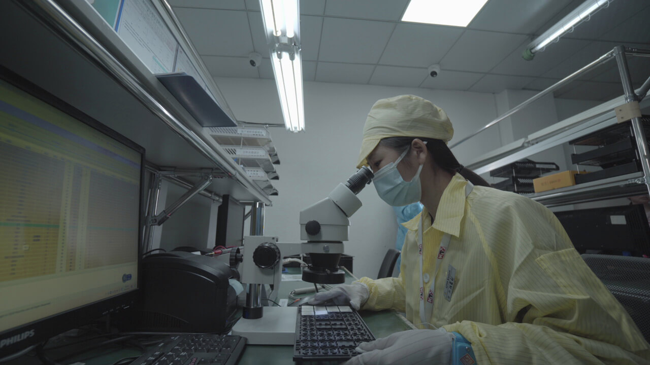
This inspection test is automated by machine and monitored by an engineer. The appliance inspects the copper sheets and compares them to the design files. If the engine finds any inconsistency between the design and the fabricated sheets, a delivered alert will notify the engineer to have a look at it.
Once all the layers pass the inspection, the facility can continue to the next PCB manufacturing step.

This stage will form the infamous printed circuit board. A multi-layer board fabricated from copper sheets blasted by a template of a beautifully designed layout and schematic. During this PCB manufacturing process, the facility will align the panels together. Once aligned, the layers bonded into a single PCB board.
The first alignment stage is done by setting the sheets on a table using heavy clamps. Those clumps will close tightly on the layers to ensure they are consistent. Any inconsistency between the layer’s positions could result in PCB fabrication failure. Once the PCB layers are aligned, it’s time to move to the bonding process, which is automated using a computer.
The bonding process starts by heating the layers to the right temperature and applying high pressure, ensuring they stick together. Then, the layers cool down, and the engineer takes them to the next PCB manufacturing stage.
PCB designs include multiple holes such as vias and other holes specified by the designer. A precise machine does the drilling process. Once attached, the machine drills the spot according to PCB’s original design. Drilling takes time. The device works slowly and precisely, ensuring no damage or cracks occur over the fabricated board.
As mentioned earlier, PCB board manufacturing uses a lot of chemicals. This process will ensure a skinny layer of copper will enter and protect the recently drilled holes. Without this step, the fiberglass in the layers will be exposed, which could result in potential damage over time. Our PCB is almost ready at this stage, but it’s not protected well enough to ensure long shelf life and durability in different conditions.
This PCB manufacturing stage is easy and quick. It’s fully monitored and controlled by computers ensuring precise and consistent results.
During the first PCB manufacturing and fabrication stages, we blasted the inner layers with UV lights to create traces on the copper using the film. This time we do the same, but instead, we operate the UV lights on the outer layer. This stage is very similar, and once the resist is hardened, the PCB board will be cleaned from any excess copper material.
The Electronics PCB manufacturing process requires applying a solder mask to protect against oxidation and prevent solder bridges from forming. Before using the solder mask, the manufacturer will ensure the board is clean and undergoes an epoxy covering process.
At this stage, we have successfully fabricated our PCB board. The last PCB manufacturing stage in pcb board making will be to note down any information such as fabrication date or text using Silkscreen. This process is done using ink-jet, and PCB manufacturers use it to write batch production timestamps on the final board. According to the PCB design, Silkscreen can indicate text, logos, and images.
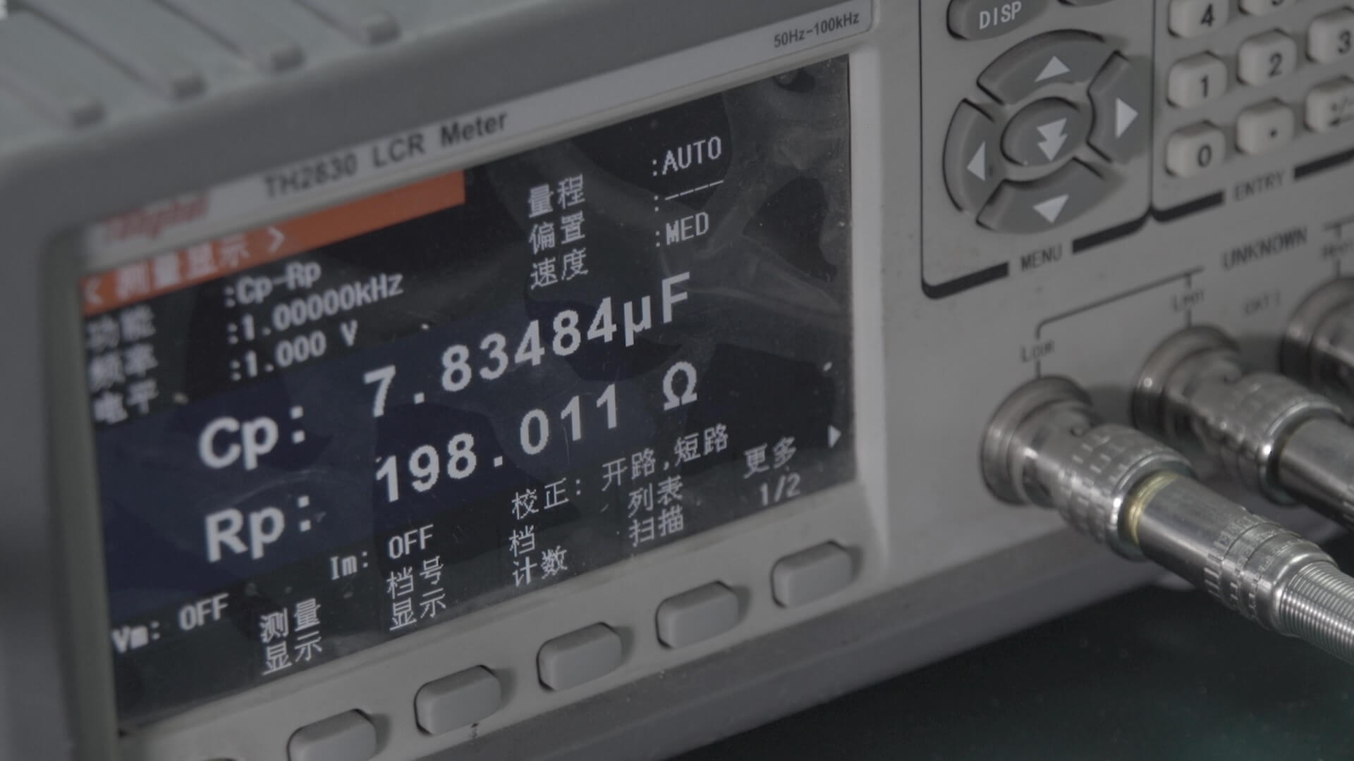
PCB maker are committed to top-quality PCB production. For that reason, an electrical test must be conducted once the board is fabricated. During this test, the PCB will be tested according to the original design. The tests include conductivity, short circuit, and other similar tests to ensure PCB’s normal function. During the test, if there are problems such as short circuits and open circuits, we have professional test engineers to carry out circuit repair to escort your project.
When the PCB production is complete, the PCB plates are cut according to the customer’s requirements. During the PCB manufacturing stages, the plates are delivered as one to ensure efficiency.
Manufacturing PCB is not easy and combines different stages at different complexity levels. PCB manufacturing requires many tools and machinery, which is usually automated. During the process, chemicals are used to ensure the protection and functionality of the PCB board over time. Whenever your board is 2 or 16 layers, PCBasic can make the process easy for you.
With over 15 years of experience manufacturing PCB, we learned how to avoid costly mistakes and ensure PCB quality over a long period.
PCB manufacturing might seem like a long process with many steps, but with PCBasic, it doesn’t have to be! Let us handle the fabrication and ensure it won’t go wrong.

Assembly Enquiry
Instant Quote
Phone contact

+86-755-27218592
In addition, we've prepared a Help Center. We recommend checking it before reaching out, as your question and its answer may already be clearly explained there.
Wechat Support

In addition, we've prepared a Help Center. We recommend checking it before reaching out, as your question and its answer may already be clearly explained there.
WhatsApp Support

In addition, we've prepared a Help Center. We recommend checking it before reaching out, as your question and its answer may already be clearly explained there.