A solder mask is one of the essential and often overlooked components of any printed circuit board (PCB). As an integral protective coating applied during manufacturing, PCB solder mask serves several important functions that ensure your circuit board functions as intended. However, for many engineers working with PCBs, a solder mask's exact purpose and role are often unknown or taken for granted.
In this comprehensive guide, we will explain in detail what a solder mask on PCB is, the different types available, and how it critically impacts the reliability and lifespan of your PCBs. Read on to learn their essential functions and why proper solder mask coverage and selection is vital for application-specific requirements.

What is A Solder Mask Layer
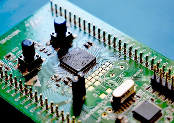
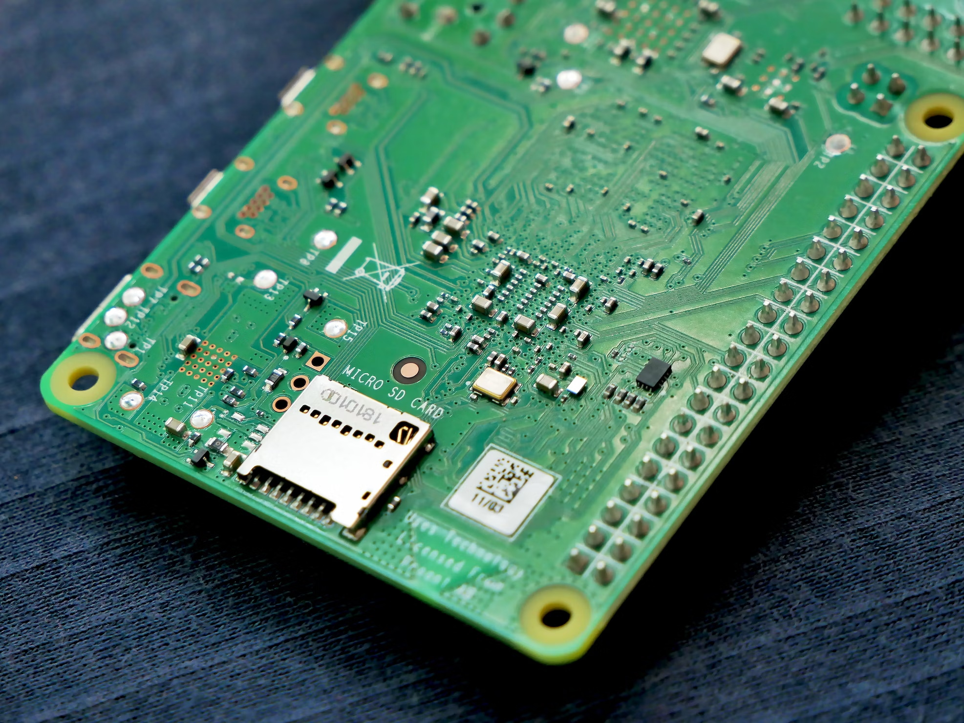
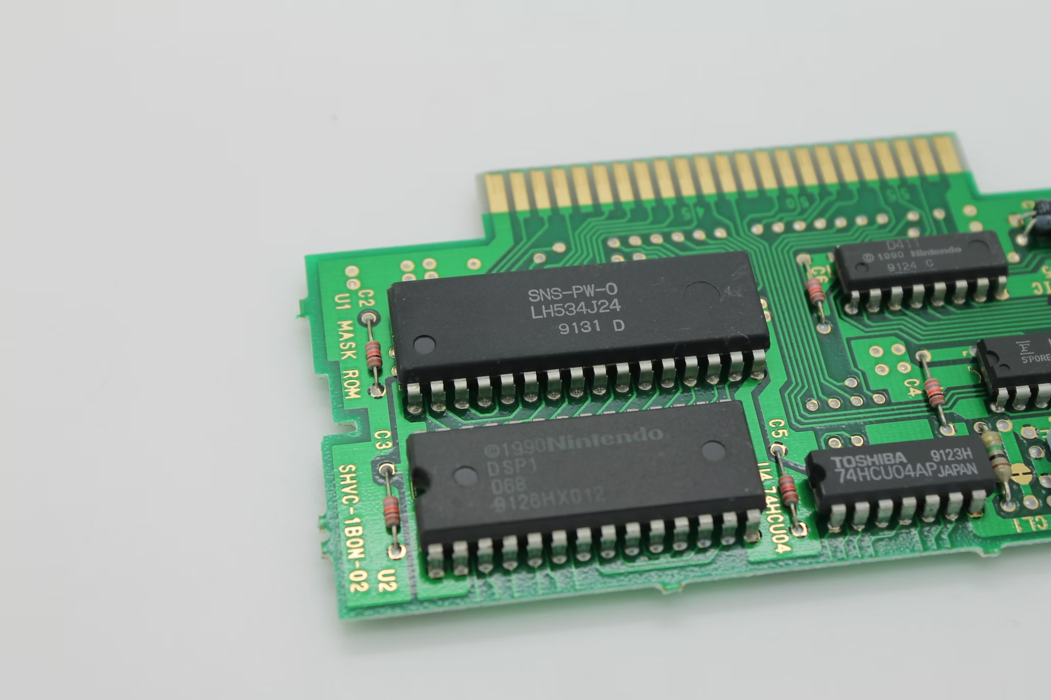
A solder mask, or solder resist, is a protective coating applied to printed circuit boards during manufacturing. This special ink-like polymeric layer prevents solder from adhering where it is not wanted. After component installation, a solder mask is screened or sprayed onto the board, covering all non-conductive areas. It includes the spaces between trace lines and pads and unnecessary inner layers.
By selectively blocking solder flow, the mask allows for uniform electrical connections between precise circuitry points during the wave or reflow soldering processes. It helps ensure long-term reliability and prevents accidental electrical shorts.

About PCBasic
Time is money in your projects – and PCBasic gets it. PCBasic is the pcb assembly company that delivers fast, flawless results every time. Our comprehensive PCB Assembly Services include expert engineering support at every step, ensuring top quality in every board. As a leading PCB Assembly Manufacturer, we provide a one-stop solution that streamlines your supply chain. Partner with our advanced PCB Prototype Factory for quick turnarounds and superior results you can trust.
Solder Mask Materials
Solder masks are typically made from epoxy, polyimide, or acrylic materials. Epoxy solder masks are the most common, providing good chemical and thermal resistance and adhesion. They are suited for general-purpose applications.
Polyimide masks have superior thermal endurance, making them suitable for aerospace and military use at higher temperatures.
Acrylic masks are more economical but offer less durability. The material selected depends on specific circuit demands and expected manufacturing and usage conditions.
Solder Mask Colors
Solder masks are usually green, which makes the circuitry features easily visible. However, you can also use red, blue, black, and white colors. Green is preferred as it offers high contrast against the typical color of PCBs.
During inspection and rework, different colored masks can simplify identifying multiple boards. They may also indicate special applications like implied ground planes or forked circuits. Custom colors are even becoming famous for product branding and style purposes. Proper coloring improves manufacturability and long-term maintenance.
Why Use Solder Mask on PCB Boards
Solder mask is an essential protective coating in printed circuit board (PCB) manufacturing. Applying a solder resist provides several key benefits:
● Insulation: The solder mask layer insulates the board and prevents shorts between closely spaced traces or pads, thus improving electrical reliability.
● Component Placement: The solder mask defines pads and areas for component placement, aiding automatic assembly.
● Solderability: The solder mask prevents oxidation on copper traces and pads, improving their solderability. It ensures solid and reliable connections.
● Contamination Protection: The coating protects against environmental contaminants and corrosion, extending the usable lifetime of the board.
●
Aesthetics: Many solder masks are green or another color, visually identifying solder and non-solder areas for quality control.
Types of Solder Mask Layers
There are different types of solder mask layers, each with its benefits. Here are the three main ones.
1. Epoxy Liquid
Epoxy liquid is a type of photosensitive liquid polymer that is commonly used as a solder mask layer. It consists of epoxy resin and a photo-initiator dissolved in a solvent. When exposed to UV light through a photomask, the photo-initiator triggers a chemical reaction that crosslinks and hardens the exposed epoxy resin.
The unexposed areas can then be washed away, leaving behind the cured patterned epoxy layer as the solder mask. This working process provides good adhesion, thermal, and chemical resistance for the epoxy liquid solder mask. It is widely used in PCB manufacturing due to its excellent insulating properties.
Pros:
● It is highly reliable
● Protection against various hazards
● Able to coat complex geometries uniformly
Cons:
● Relatively high material and processing costs
2. LPSM/LPI
LPSM (Liquid Photo-imageable Solder Mask) uses a liquid photo-imageable (LPI) polymer material as the solder mask layer. The LPI consists of an epoxy-based liquid resin mixed with a photo-acid generator. When exposed to UV light through a photomask, the photo-acid generator produces an acid to catalyze the crosslinking reaction of the resin.
The unexposed areas can then be developed away, leaving behind the cured patterned LPI solder mask layer. This light-sensitive, liquid-based working process allows LPI solder masks to uniformly coat PCBs with fine geometries and features.
Pros:
● Offers good adhesive strength to the PCB
● It has excellent chemical and thermal resistance
Cons:
● Strict environmental controls needed for the photolithography process
3. DFSM
DFSM (Dry Film Solder Mask) is a photosensitive laminate material used as a solder mask layer. It consists of photosensitive epoxy or polyimide resin sandwiched between polymer films.
The working process involves laminating the dry film onto the copper-clad board under heat and pressure. This bonds the resin layer to the board. It is then exposed to UV light through a photomask, which hardens the resin in the defined pattern. Development removes the unexposed areas, leaving behind the cured solder mask pattern.
The critical advantage of DFSM is that it is a dry film process. This means it does not require the use of any solvents during application and development. It provides good insulation properties and adhesion to the board, like liquid resins.
Pros:
● Solventless process
● Uniform thin film thickness
● Easy handling and registration
● Good insulation and adhesion
Cons:
● It's hard to coat complex board shapes/geometries uniformly

Other Terminology You Should Know About Solder Mask
When working with solder masks, there are a few other key terms you should be familiar with:
● Tented Vias: It is how the solder mask is applied over plated through holes (PTH) or vias on a PCB. Instead of the solder mask being fully set into the hole, it tents or domes slightly over the holes, which helps prevent solder bridges from forming between closely spaced holes or vias during assembly.
● Solder Mask Clearance: This refers to the small gap left between the edges of the solder pad areas and the solder mask material. This clearance is essential to ensure the solder has a clean area to properly wick and flow during reflow without being inhibited by the mask. It is usually a minimum of 100 micrometers around each pad.
● Solder Mask Opening: It is where the solder should be deposited and components attached. They are where the solder mask layer is absent, exposing the bare copper pads and circuitry below. Precise openings aligned with the pad areas are critical for reliable solder joints.
● Solder Mask Expansion: This refers to extending the mask slightly beyond the defined pad areas or edges of the circuit features. This small amount of overhang helps prevent solder bridging or short circuits between closely placed pads or traces during the assembly process. It provides a gap or boundary for the molten solder.

What Solder Mask Should You Use on Circuit Boards
When selecting a solder mask layer for your PCB, there are a few fundamental properties and considerations to keep in mind.
Chemical Resistance
The solder mask needs to resist chemical attacks from the soldering and assembly process. Look for a mask that can withstand exposure to solder flux, solvents for cleaning, and other chemicals used during manufacturing and service. Epoxy solder masks typically offer excellent chemical resistance.
Adhesion
The mask layer must adhere tightly to the substrate and copper traces. Proper adhesion ensures the mask does not peel or bubble during manufacturing or use. Both dry film and liquid photo imageable solder masks commonly deliver strong adhesion if fully cured.
Dielectric Strength
The dielectric strength impacts electrical insulation. A high dielectric constant helps prevent track migration and shorting. Most solder masks used on commercial boards have a dielectric constant above 3, though some specialized high-density designs require an even higher value.
Colorfastness
The mask color should not fade or discolor from heat, humidity, or UV exposure over time. Green is a popular color as it is very colorfast. Be sure to verify the lightfastness rating if appearance is important over the long term.
Choosing a solder mask that performs well across these key properties will result in reliable, long-lasting protection for the circuit traces on your PCB. Consider samples from leading suppliers like PCBasic to find the best match for your application needs and environment.
Solder Mask Design Guidelines
When designing PCBs, the solder mask plays an essential role in protection and functionality. Following some key guidelines will help ensure your solder mask effectively supports your circuit board design.
Leave a Gap Between Solder Mask and Pads/Components
Always leave a small gap between the solder mask and the components or copper pads it covers. This gap, typically 0.005 inches, prevents the mask from bridging or coming into contact with the pads, which could cause defects. It also creates a pathway for the solder to flow and properly adhere.
Do Not Place Solder Mask Over Anneal Lines
Be sure not to place the solder mask over any anneal lines on the PCB. Anneal lines help relieve stress on the board and should remain free of any covering. Solder masks over annealing lines can fracture during the manufacturing process.
Use Gradual Radius Edges for Slots and Openings
Verify any slots or openings in the solder mask have rounded corners and gradual tapered edges. Sharp inside angles or corners are prone to cracking, possibly exposing the underlying copper. All edges should have a minimum 0.002-inch radius.
Maintain Consistent Solder Mask Thickness
Be sure to maintain a consistent solder mask thickness. Variations can lead to Bridging, while a thinner coat may fail to isolate pads fully. A thickness between 0.0015-0.002 inches appropriately balances protection and manufacturability.
How is Solder Mask Applied on PCB
Applying solder masks correctly and consistently is an important part of PCB manufacturing. Here are the typical steps involved in applying solder mask on PCBs:
Step 1: Surface Preparation
The PCB first goes through a degreasing process to remove any impurities on the copper surface, such as oil, grease, or other contaminants. This is typically done using solvents in an automated degreasing machine or manually with degreasing chemicals. Thoroughly cleaning the surface is important for proper adhesion of the solder mask.
After degreasing, a chemical etchant like sulfuric acid is applied. This etches away a very thin top layer of the raw copper cladding, mechanically roughening the surface at a microscopic level. This provides more anchoring points for the solder mask to grip onto. The board is then rinsed with water to remove any remaining etchant residues. Some manufacturers may include an additional ionized water rinse to further cleanse the copper at an atomic scale before drying.
Step 2: Apply the Solder Mask (Lamination and Screen Printing)
Once clean and etched, the copper surface is prepared for solder mask application. Lamination and screen printing are the two primary methods used.
For screen printing, a photosensitive emulsion is applied to a tightly woven mesh screen according to the pad and trace pattern of the PCB design. It is then UV-exposed to harden the emulsion in the open print areas. A liquid solder mask is poured onto the screen surface, and a squeegee blade forces it through these openings. This deposits the mask onto the board below over multiple passes to build up the necessary coverage.
In lamination, a dry film of the photosensitive solder mask material is bonded as a sticker to a backing liner similar to transfer tape. Large sheets are cut using a plotter or laser to match individual board patterns. The film is solder-side down onto the prepared copper and fed through a heated laminator. Pressure and heat activate the adhesive, tightly fusing the dry film resin to the PCB below.
Step 3: Drying/Curing
The curing method varies slightly based on the application type in Step 2 above. Screen-printed liquid masks are loaded onto conveyor dryers or racks and fed through a curing oven or drying tunnel. Temperature is slowly ramped to drive off solvents without bubbles or defects forming.
Dry film masks placed on PCBs are cured by controlled photo or thermo processes like UV lamps or heating plates to complete the crosslinking reaction. This ends up forming the final solid coating. Proper curing ensures the solder mask is fully hardened and ready for further processing.
Step 4: Inspection
Automated optical inspection (AOI) machines carefully examine the finished solder mask coating for flaws or deficiencies. High-resolution cameras detect issues like voids, bridges between traces, or stains that could compromise protection. This ensures the quality meets specifications before further assembly. Any problem areas identified may require a touch-up application to fix.
Step 5: Drill Mask If Required
Drill Masking, an additional solder mask coating, is sometimes applied over plated through-hole (PTH) drill holes after the main application. This prevents solder from wicking or drawing into the holes during the surface mount assembly process, which could cause defects. The drill mask liquid is precisely screen printed only over the holes using the same basic techniques as the main solder mask process.
Step 6: Marking/Finishing
Identification markings may be added if the customer requires them. This commonly involves screen printing labels, logos, or traceability codes directly onto the solder-masked surfaces using special markings inks.
Surface finishing, like tin-lead plating, is sometimes applied at this stage to enhance solderability before component placement. The fully processed, inspected, and marked boards are prepared for final packaging and shipping to the customer or the next assembly stage.
IPC Standards for Solder Mask on PCB
Proper solder mask application and features are crucial for manufacturability and reliability. IPC has established several standards to guide solder mask specification and testing.
● IPC-SM-840 outlines requirements and test methods for liquid photo-imageable solder mask materials. It covers items like recommended film thickness, curing temperature, adhesion properties, and resistance to solvents.
● IPC-SM-781 covers standard electrical and physical tests for solder masks. This includes inspection of pinhole and void defects, pad cratering, filleting, and impact resistance. Correct solder mask coverage helps prevent short circuits.
● IPC-SF-818 establishes guidelines for solder mask definitions and abbreviations. This standardizes terminology for features like solder mask color, legend alignment, and other attributes. Consistent language prevents specification errors.
●
IPC-1791 defines preferred solder mask expansion ratios based on board design rules. The right ratio prevents solder bridging between closely spaced pads during reflow.
Common Solder Mask Defects and Their Causes
Like any manufacturing process, solder masking is susceptible to defects impacting quality and reliability. Here are some of the most common defects.
● Solder bridging: Occurs when the solder flows between two closely spaced contacts or pads, causing an electrical short. It is often caused by too much solder paste being applied, flux traces left on the board, or inadequate cleaning after soldering.
● Pinholes: Pinholes are small holes or gaps in the solder mask layer that expose the underlying copper. They can be caused by contamination during solder mask application or inadequate curing. Pinholes allow the solder to wick underneath during reflow, potentially causing shorts.
● Peeling/Delamination: Peeling or delamination of the solder mask occurs when the mask layer separates from the board material. It is usually due to inadequate surface preparation of the board before solder mask application or incompatible board and solder mask materials. Peeling exposes copper that can oxidize and lead to poor solder joint formation or electrical issues over time.
●
Missing Solder Mask: Areas where the mask is completely absent leave copper fully exposed. This is often due to imperfections during the application process, such as clogged stencils. It allows the solder to wick onto exposed copper structures during reflow.
FAQs About Solder Mask Layer
1). Can You Make a PCB Board Without a Solder Mask?
Technically, it is possible to make a PCB without a solder mask layer. However, it is not recommended as the solder mask provides important functions. Without it, solder may wick into neighboring traces and pads, potentially causing shorts. It also protects the board and makes it easier to see traces and pads.
2) What is the Paste Layer on PCB?
The paste layer refers to the solder paste applied to the PCB during surface mount assembly. Solder paste is a mix of small solder alloy balls in a sticky flux vehicle. It is applied evenly using a stencil to transfer the paste to the component pads on the PCB in the desired patterns.
3) Does the Solder Mask Color Matter?
The solder mask color is not functionally important, but certain colors like green are commonly used as they provide good contrast to see traces and pads. Dark colors like black can make traces harder to see. Lighter colors like yellow or white may show defects or damage more easily.
4) What are the Disadvantages of Solder Masks?
Potential disadvantages include:
● Cost/time to apply the mask.
● Risk of defects from the application.
● Risk of the mask flaking off over time.
● Difficulty inspection under mask areas.
● Make reworking areas harder by covering up traces and pads.
5) Does a Solder Mask Repel Solder?
Yes, a key function of a solder mask is to repel solder. It is formulated with materials that prevent solder from adhering to the surface. This controls where soldering occurs and prevents unintended bridging between close pads/traces.
6) How Thick Should a Solder Mask Be?
The recommended thickness for a solder mask is 20-50 microns. Thinner than 20 microns may not provide enough protection, while thicker than 50 microns offer no real benefits and make traces harder to see under the mask. The most suitable is 25-35 microns for a good balance of properties and visibility.
7) What Solvent Removes the Solder Mask?
Common solvents that remove solder masks include Alcohol (IPA), Acetone, and MEK (Methyl Ethyl Ketone). Nail polish remover also works in many cases. The mask material needs to be sufficiently dissolved/softened by the solvent to be removed without damaging underlying copper traces/pads.
8) How Do You Apply the Solder Mask Evenly?
Solder masks are commonly applied using screen printing or spinning processes. Screen printing uses a fine mesh stencil to scrape/squeegee the liquid mask material over the PCB in a controlled thickness. Spinning evenly distributes the liquid across the board using centripetal force. Proper masking material rheology, process control, and cleaning are keys to an even application.
9) When Do You Need a Solder Mask Touch-up or Reapplication?
Solder mask reapplication may be needed if the original mask becomes damaged, cracked, flaked, or worn away in production/usage. Touch-ups can fill in small defects. Reapplication would be done if large areas are compromised. Other causes could include rework processes, condensation/cleaning chemical exposure over time, or long-term environmental exposure degrading the mask.
Conclusion
Solder mask plays a crucial role in protecting PCB circuits and preventing shorts. Whether you're designing prototypes, manufacturing products, or troubleshooting boards, an understanding of solder masks will serve you well.
For your next project, consider sending your Gerber files to PCBasic. As a leading PCB manufacturer and assembly house, we can produce boards for you with precision-applied solder masks. Our experienced technicians and quality processes ensure every project is done right. Contact us today to discuss your circuit board needs and get a fast turnaround on a prototype or production run.
Looking for a PCB or PCBA quote? Contact us now.
