Global high-mix volume high-speed PCBA manufacturer
9:00 -18:00, Mon. - Fri. (GMT+8)
9:00 -12:00, Sat. (GMT+8)
(Except Chinese public holidays)
Global high-mix volume high-speed PCBA manufacturer
9:00 -18:00, Mon. - Fri. (GMT+8)
9:00 -12:00, Sat. (GMT+8)
(Except Chinese public holidays)
HomePage > Blog > Knowledge Base > A Comprehensive Guide to Barebones PCBs
In electronic products, printed circuit boards (PCBs) are core components. Whether it is a mobile phone or a medical device, PCB is indispensable inside. Although the final products use the assembled circuit boards, in the early stage of design or when making prototypes, engineers usually use simpler boards, such as barebones PCB, bare PCB and zero PCB.
This article will focus on introducing the barebones PCB, explaining its functions, features, common uses, and making a comparison between it and the bare PCB as well as the zero PCB. Whether you are just getting started with electronic design or are an experienced engineer, understanding these basic circuit boards will help you choose the appropriate development plan.
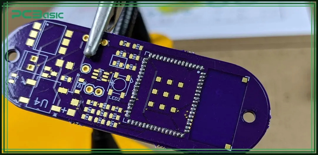
A barebones PCB is a simplified circuit board, which only includes the most basic copper traces and layout. It does not add solder mask, silkscreen or any other protective layer during the manufacturing process. This means that the copper traces and solder pads on the board are exposed, which makes it more convenient for engineers to conduct manual soldering and prototype verification in the early stage of development.
Unlike fully assembled PCBs, barebones PCBs are not suitable for finished products, but they are a low-cost platform for verifying circuits and test routing.
The design of barebones PCB is very simple, eliminating many additional processing steps in conventional circuit boards. It has several remarkable features:
• No solder mask: The green or other colored coatings we usually see are solder mask layers, which can protect the circuits and prevent short circuits. In the barebones PCB, this layer is removed, eliminating the related process.
• No silkscreen: Generally, circuit boards are printed with component numbers, polarity symbols and other marks to assist in assembly, which is called silkscreen. Barebones PCBs do not contain this printed information and appear cleaner in appearance, but it also means that extra care must be taken to identify the positions of components during assembly.
• Exposed copper: As there is no protective layer, the copper traces and pads on the circuit board are directly exposed. This design makes it more convenient for engineers to solder, test and modify with hand tools.
• Lower cost: By eliminating the production steps of the solder mask and silkscreen, the processing flow of the entire board becomes simpler, thereby significantly reducing the production cost.
• Faster turnaround: Because the manufacturing process is shorter and faster, the lead time of barebones PCBs is shorter than that of common PCBs, making them highly suitable for urgent projects or rapid prototyping.
It is precisely because of these characteristics that barebones PCBs are widely used in the early stages of product development, teaching experiments and DIY projects. It provides electronic engineers and enthusiasts with a fast, practical and low-cost way to verify circuits.
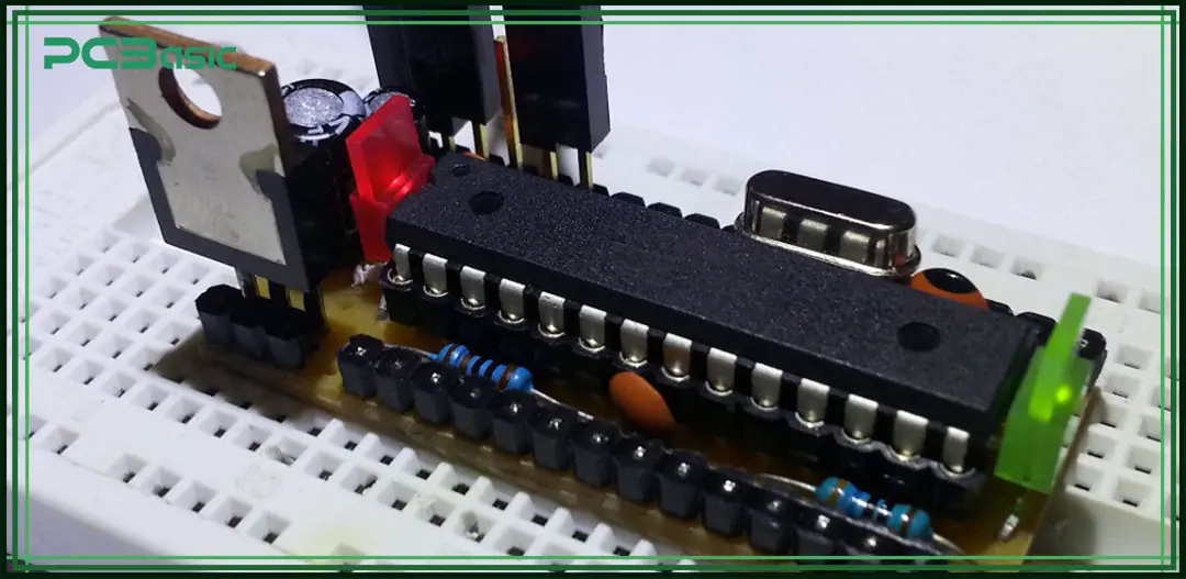
Barebones PCBs are widely used in situations where cost, efficiency and accessibility take precedence over durability or appearance. Common applications include:
• Prototype testing: Ideal for initial design validation.
• DIY electronics: Popular with makers and hobbyists.
• Educational kits: Used in teaching electronics fundamentals.
• Low-volume production: Suitable for early-stage product development.
Although barebones PCBs are not suitable for harsh environments or long-term use, they play a key role in driving product innovation.
 About PCBasic
Time is money in your projects – and PCBasic gets it. PCBasic is a PCB assembly company that delivers fast, flawless results every time. Our comprehensive PCB assembly services include expert engineering support at every step, ensuring top quality in every board. As a leading PCB assembly manufacturer, we provide a one-stop solution that streamlines your supply chain. Partner with our advanced PCB prototype factory for quick turnarounds and superior results you can trust.
In prototype development, teaching experiments or cost-sensitive projects, choosing a suitable circuit board is of vital importance. Barebones PCBs have become the first choice for many engineers and electronics enthusiasts because of their simplicity, efficiency and environmental friendliness. The following are three main advantages:
• Barebone PCB– Lower costs
The greatest advantage of using barebones PCBs is that they are cheap. Because they eliminate the solder mask and silkscreen printing on conventional PCBs, less material is used in the manufacturing process and the process is simpler. This not only reduces the unit price of each board, but also saves the production cost of the entire batch. It is particularly attractive for development projects with limited budgets.
• Barebone PCB– Saves Space
Because there are no additional layers, the barebones PCB is more compact and flexible in structure. This design is suitable for small equipment or modules with limited space. It also makes it convenient for engineers to directly modify the circuit on the board, such as adding a patch cord or replacing the solder pad, without worrying about the solder mask layer blocking or affecting the operation.
• Barebone PCB– More Eco-friendly
Traditional PCB manufacturing involves various chemical processes such as coating, developing, and etching. These steps not only consume time and materials but also generate chemical waste. In contrast, a barebones PCB skips many of these additional steps, reducing the use and discharge of chemicals as well as lowering energy consumption. This makes it more environmentally friendly while still fulfilling basic functional requirements, aligning with the trend toward greener manufacturing.
If you want to quickly build circuit prototypes, conduct small-batch tests, or just undertake an informal electronic project, a barebones PCB is an extremely cost-effective choice.
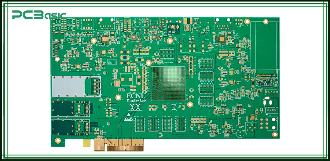
Although many people confuse bare PCBs, zero PCBs and barebones PCBs in daily communication, in fact, they are three different types of circuit boards, each with different structural characteristics and application scenarios. Understanding the differences between them can help you make more accurate choices during the design, development, or procurement process.
Bare PCB
The bare PCB refers to a circuit board that has not yet been soldered with any components. It usually completes the standard manufacturing process. It has a complete solder mask layer and a silkscreen layer. You can regard it as a circuit board that is ready for assembly but only lacks the mounting components. This type of board is suitable for the pre-assembly stage of most formal projects. It can be a single-layer board or a complex multi-layer board.
Zero PCB
Zero PCB is a kind of universal circuit board with pre-drilled holes. It has regularly arranged holes and copper-clad areas and is suitable for building simple circuits by hand. It usually has no preset circuit diagram, nor any protective layer or marking. It is more like a blank platform for electronics enthusiasts to play freely. This type of board is often used in student experiments, DIY projects or for quickly verifying some basic circuit principles.
Let’s compare the three different boards on a chart comprehensively:
|
Feature |
Bare PCB |
Zero PCB |
Barebones PCB |
|
Solder Mask |
Usually present |
Absent |
Absent |
|
Silkscreen |
Usually present |
Absent |
Absent |
|
Copper Layout |
Custom |
Generic grid |
Custom |
|
Component Mounting |
For reflow/wave soldering |
Manual |
Manual |
|
Application |
Pre-assembly stage |
Breadboarding |
Prototyping |
The barebones PCB is a simple and cost-effective solution in prototype development. It has no solder mask layer or silkscreen printing, making the early design verification process faster and less costly. Compared with bare PCBs and zero PCBs, barebones PCBs simplify the manufacturing process while maintaining the custom layout.
If you are a hardware developer, a student or an electronics enthusiast, mastering the usage skills of barebones PCBs will save you a lot of time and money. Just keep in mind: Each project has different requirements. Understanding when to choose bare PCBs, when it is sufficient to use zero PCBs, and when to use barebones PCBs can make your efforts more efficient.
Assembly Enquiry
Instant Quote
Phone contact

+86-755-27218592
In addition, we've prepared a Help Center. We recommend checking it before reaching out, as your question and its answer may already be clearly explained there.
Wechat Support

In addition, we've prepared a Help Center. We recommend checking it before reaching out, as your question and its answer may already be clearly explained there.
WhatsApp Support

In addition, we've prepared a Help Center. We recommend checking it before reaching out, as your question and its answer may already be clearly explained there.