Global high-mix volume high-speed PCBA manufacturer
9:00 -18:00, Mon. - Fri. (GMT+8)
9:00 -12:00, Sat. (GMT+8)
(Except Chinese public holidays)
Global high-mix volume high-speed PCBA manufacturer
9:00 -18:00, Mon. - Fri. (GMT+8)
9:00 -12:00, Sat. (GMT+8)
(Except Chinese public holidays)
HomePage > Blog > Knowledge Base > What is DIP?
In the previous article, we introduced to our readers what is SMT (surface mount technology). We also covered the advantages of SMT and the standard process of SMT assembly.
We also learned that the SMT chip process is often used during mass production in the PCBA chip processing industry. It is very convenient for use in various advanced electronic products and equipment, including notebook computers, etc …
In today’s world where electronic products are gradually becoming smaller, can SMT completely replace DIP? At the end of this article, you’ll be able to answer that question for yourself. But first, let’s explain what DIP stands for.
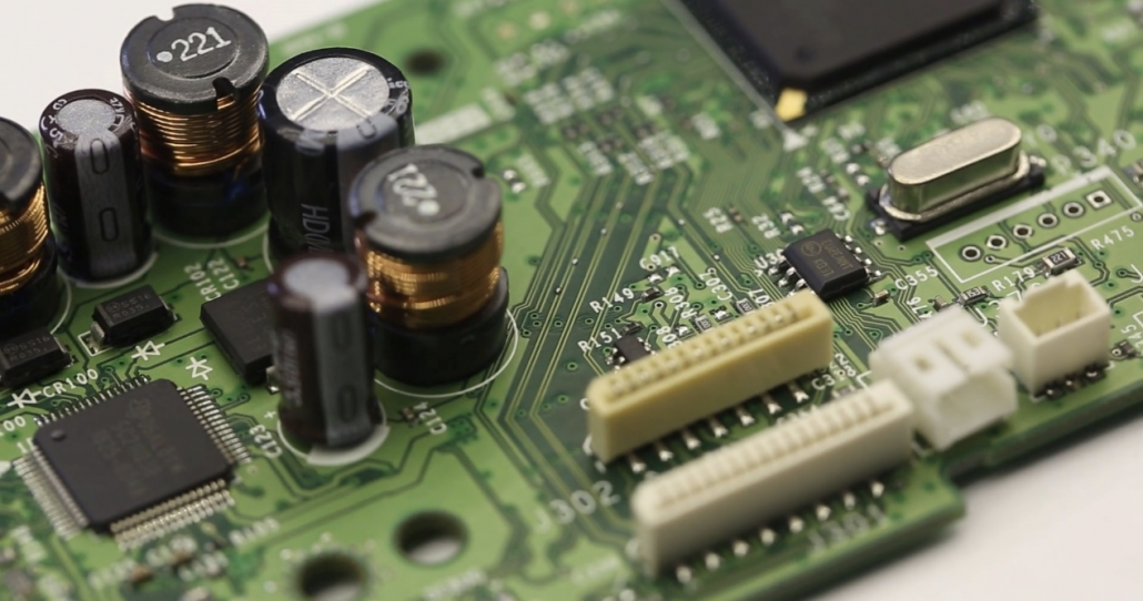
In simple terms, SMT uses “sticking” technology while DIP “plugged-in”. DIP electronic components have two rows of pins. Soldering those pins done by inserting the two rows of pins into the soldering positions according to the number of solder via holes in pcb.
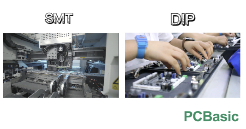
In our previous article, we listed the advantages of SMT processing in PCBA. And the advantages are obviously vast. If that’s the case, why use DIP processing technology? Here are some of the reasons:
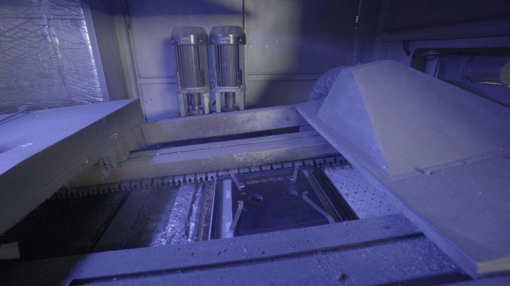
When assembling DIP components, the pump continuously sprays liquid tin waves to form solder wave crests. When the circuit board on the conveyor belt enters at a certain speed, the solder overflows to the surface of the circuit board in the form of wave peaks while welding the solder joints of the plug-in material. This technique is called wave soldering.
In PCBasic, the standard DIP assembly process is as follows:
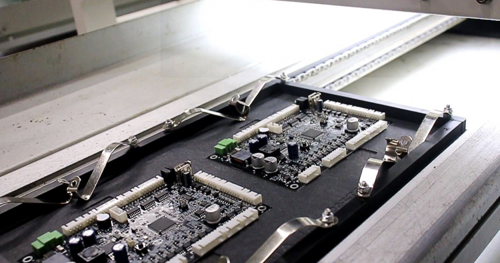
For many reasons DIP still plays an important role in the PCBA electronic processing industry. Compared with the automation of SMT, the DIP plug-in requires a large-scale manual operation that needs a lot of human labor. In theory, because of the high proportion of labor, the defect rate of DIP will be relatively high. Therefore, while doing DIP processing it’s crucial to monitor and guarantee the quality of the PCBA.
Like every project, DIP also has its own precautions that must be considered before the processing begins:
The answer is: that SMT patches cannot completely replace DIP processing.
SMT and DIP are both important parts of PCBA processing, but not all PCBA manufacturers have SMT placement capability and DIP post-soldering capability, and the processing quality is difficult to guarantee.
When choosing a PCBA partner, we recommend conducting an on-site inspection of the processing factory.
PCBasic also provides you with factory inspection services. If you cannot come in person, we can provide you with an online real-time factory inspection at any time. If you have a custom pcb assembly need or request, we have the power to fulfill it for you.

Assembly Enquiry
Instant Quote
Phone contact

+86-755-27218592
In addition, we've prepared a Help Center. We recommend checking it before reaching out, as your question and its answer may already be clearly explained there.
Wechat Support

In addition, we've prepared a Help Center. We recommend checking it before reaching out, as your question and its answer may already be clearly explained there.
WhatsApp Support

In addition, we've prepared a Help Center. We recommend checking it before reaching out, as your question and its answer may already be clearly explained there.