Global high-mix volume high-speed PCBA manufacturer
9:00 -18:00, Mon. - Fri. (GMT+8)
9:00 -12:00, Sat. (GMT+8)
(Except Chinese public holidays)
Global high-mix volume high-speed PCBA manufacturer
9:00 -18:00, Mon. - Fri. (GMT+8)
9:00 -12:00, Sat. (GMT+8)
(Except Chinese public holidays)
HomePage > Blog > Knowledge Base > The most complete guide to PCB basics
Ever wanted to learn about how to get started with PCB but didn’t know how? In this article, we will walk through the basics of PCB design. We will cover the topics of what is PCB and where was it first used. By the end of this article, you might even be able to design PCB by yourself!
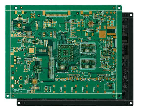
PCB consists of a copper board made of insulating material with conductive pathways etched on it. The PCB board connects and controls electronic components in multiple devices and equipment. Such devices include computers, smartphones, televisions, and almost anything else we use in our daily lives.
PCBs consist of metal layers and insulating layers. In the fabrication process, the manufacturer solders the components to the metal layers and connects them by the conductive pathways. These pathways allow electrical signals to flow, enabling the components to work together and perform the device’s intended functions.
The PCB board industry exist for over 100 years. Over time, PCB technology has evolved to become smaller, more complex, and more sophisticated. This evolution is due to the increasing demand for more advanced technology and manufacturers.
In the 1950s, mass production of PCBs became possible, leading to the widespread use of these boards in electronic devices. As technology advanced, PCBs grew smaller, more intricate, and could accommodate more components. This paved the way for the development of the modern computer and other high-tech devices.
Today, PCBs are an integral part of modern electronics and continue to evolve to meet the demands of an ever-growing and changing industry.

circuit boards come in three main types: single-sided, double-sided, and multi-layer.
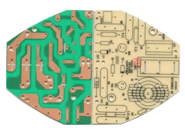
single sided pcb board have conductive pathways on one side only and are the simplest and most economical type. They are used in basic electronic devices like calculators and alarms.
Double-sided PCBs have conductive pathways on both sides and offer more complex circuit designs. They are used in devices such as desktop computers and DVD players.
Multi-layer PCBs have three or more layers of conductive material and offer even greater design flexibility. The multi-layers provide a solution when a single layer is just not enough. Often high-tech devices such as smartphones and laptops use a multi-layer PCB design due to their compact size and increased functionality.
The type of PCB used in a device is determined by the complexity of the circuit design, the size of the device, and the desired functionality.
Choosing the right PCB board CAD software can greatly impact the efficiency and accuracy of the design process. The software should meet your specific needs, including compatibility with your design process, the complexity of your designs, and the type of components you use.
When selecting circuit board CAD software, consider the following factors:
There are many types of PCB cad software available. Some of them are free and open source and some of them are paid. At the end of the day, the decision of whether to choose one CAD software over another is up to the project. Some projects are more complex while others are very simple. Just getting started with PCB design? Choosing to work with open-source CAD software will be a good idea.

Designing a PCB board involves several critical considerations. These include the schematic design, component placement, routing, and signal integrity.
The first step of PCB design is the schematic. The schematic is considered to be the “brain” behind the PCB design. This step comes after selecting the proper components. Once the components have been choosen, it’s time to draw the schematic and the logic of the circuit board.
The schematic shows the components and their connections, making it easy to visualize the flow of electrical signals between the components. It should be easy to read and clearly indicate the electrical connections between the components.
The design process that comes before starting to work with CAD software is a critical step in creating a successful PCB. A well-designed schematic can help to ensure that the PCB is electrically sound, providing a foundation for the rest of the design process. Well-organized, easily readable, and accurately represented electrical circuits in schematics reduce the risk of errors and enhance the efficiency of the design process.
Component placement is a vital aspect of designing a PCB. The designer places the components in such a way that the electrical signals can flow between them. Thus, ensuring the proper functioning of the circuit. There is also the designer who must consider factors such as the physical size and shape of the components.
There are other factors such as the space requirements for components and possible enclosure of the device. The placement of components has a significant impact on the routing of the electrical pathways. The PCB engineer should plan the routes properly to ensure layout optimization for efficient signal flow.
Placement, often called PCB layout, involves the process of taking components and arranging them on the board. The second part of the process is to connect the wires between each and every component. The wires connection process is called routing, as in building bridges and routes between the components.
Proper component placement is crucial for ensuring the quality, reliability, and performance of the PCB board and the devices that it powers.
Signal integrity is also crucial to the functionality of the circuit, and designers must ensure that signals are strong enough to reach their intended destinations. This may involve the use of decoupling capacitors, ground planes, and shielding to mitigate signal interference.
Optimizing the design for the manufacturing process, including drilling and etching, is a critical step for PCB designers. When you design your own PCB, you should always consider the use case scenarios. Different printed circuit boards have different operation requirements and conditions to be met.
The material used in PCB board manufacturing is critical to the performance and reliability of the circuit board. The two main materials used in PCB production are the base material and the conductive material.
Printed circuit boards (PCBs) typically use fiberglass or other insulating materials as their base to provide structural support. Designs choose Conductive materials during the PCB design process. Materials that conduct electricity, such as copper, create electrical pathways which are crucial to transfer signals across the PCB.
Choosing the right materials for the base and conductive layers depends on the intended use of the PCB and its operating environment. Normally, high-temperature environments require different types of pcb materials than low-temperature environments.
The material must be chosen to ensure that the board meets the electrical and mechanical requirements of the device. It must be able to withstand the manufacturing processes, including drilling and soldering. The materials should also meet all the regulatory requirements. Those requirements are often related to fire safety and environmental impact.
The fabrication of circuit boards involves several processes, including drilling, etching, and soldering.
Drilling involves creating holes in the board to accommodate the components. The holes must be precise to ensure that the components fit correctly and the electrical connections are reliable.
Etching involves removing the unwanted copper from the board to create the conductive pathways. This process uses chemical etches or laser etches to remove the copper, leaving behind the desired pattern.
Soldering involves attaching the components to the board and connecting them to the conductive pathways. PCB board manufacturers can use wave soldering, reflow soldering, or manual soldering for the soldering process. The choice of soldering method will depend on the type of component, the type of PCB, and the desired final product.
To guarantee high-quality and reliable circuit boards, manufacturers carefully control the drilling and etching processes to meet the correct specifications.
Learning PCB design without proper education and knowledge in the field is hard. The process involves years of studies and preparation, testing, and a high learning curve.
If electronics is your hobby and you’d like to learn an extra skill, designing a PCB by yourself would be a great way to learn.
For industrial and commercial use, you might need proper guidance and support.
PCBasic has years of experience in PCB design, schematic and layout customization, manufacturing, PCB and PCBA production, and much more. If you are new to PCB design or want to take your existing designs to the next level, don’t hesitate to reach out, we are here to help.

Assembly Enquiry
Instant Quote
Phone contact

+86-755-27218592
In addition, we've prepared a Help Center. We recommend checking it before reaching out, as your question and its answer may already be clearly explained there.
Wechat Support

In addition, we've prepared a Help Center. We recommend checking it before reaching out, as your question and its answer may already be clearly explained there.
WhatsApp Support

In addition, we've prepared a Help Center. We recommend checking it before reaching out, as your question and its answer may already be clearly explained there.