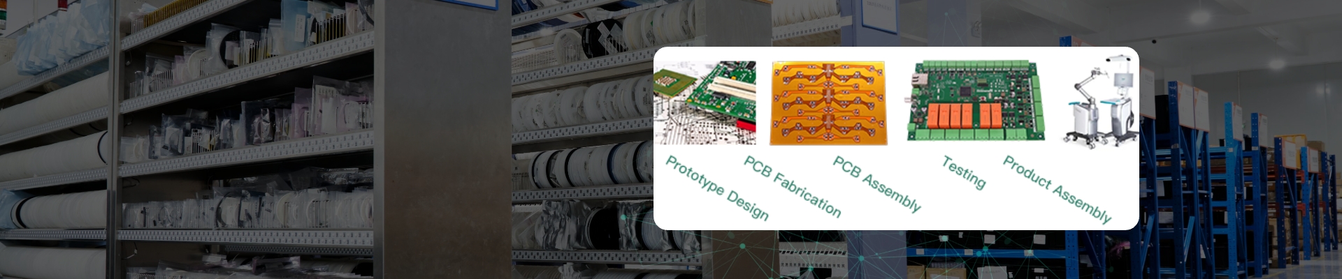
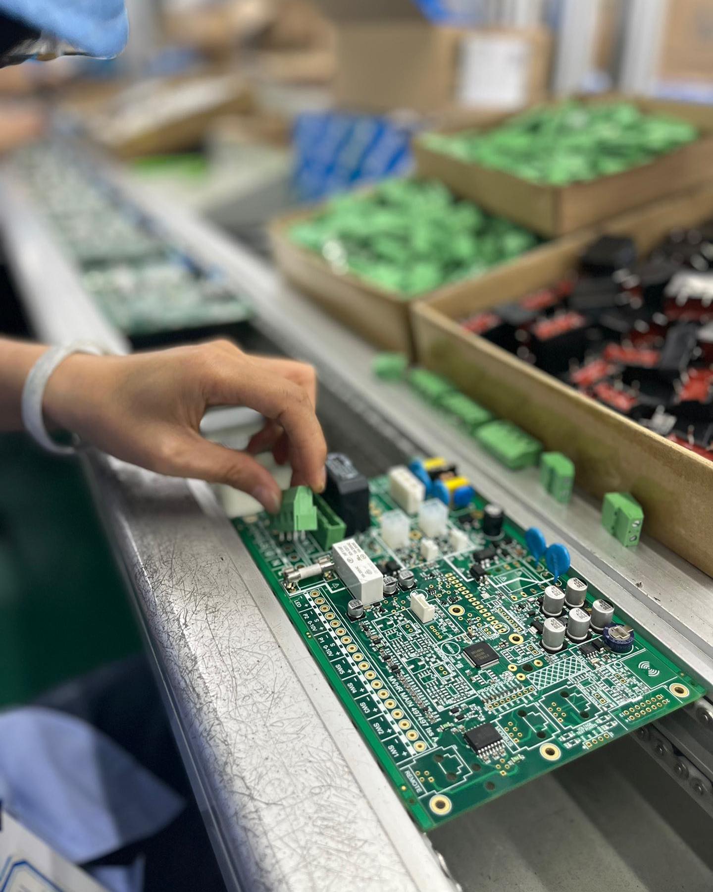
What is Single sided PCB?
Single sided PCB ’s earliest industrial application can be traced back to the early
1950s. Because of its simple design principle and manufacturing process, it occupies an
important position in the history of PCB manufacturing.
Single sided PCB is covered with
copper on one side only, with components distributed on one side and circuits
distributed on the other side. From top to bottom, single panel usually consists of
soldermask layer, copper layer and insulating material in turn.
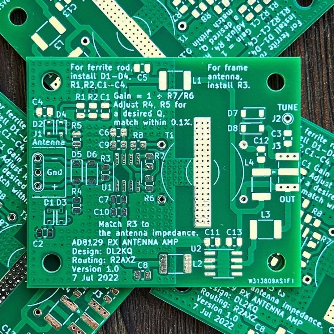
Features of Single sided PCB
As only one side of single sided PCB can distribute circuits, and the two sides can't be
connected, compared with other PCBs, they need a larger area to carry the same number of
components, so they are more suitable for the design with lower requirements for
component distribution density.
Although single layer PCB design is simpler than other types of PCB, based on the
characteristics of single-sided distribution, it has stricter specifications for the
design of wiring and component positions. For example, the pad of single sided PCB must
be large, otherwise it is easy to cause problems during welding and repair. The wiring
of the circuit board can not cross, but can only be designed along their own paths, etc.
Main applications of single sided PCB
At present, the terminal products using single sided PCB mainly include calculators,
charging products, LED lamp boards, FM radio, timers, etc. At the same time, according
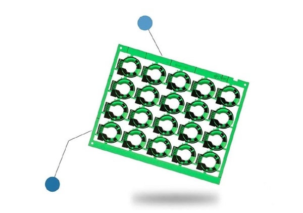
to different technology types, it can be divided into single-sided hard board, flexible
single board, soft-hard combined single board and single-sided aluminum substrate.
Advantages and disadvantages of single
sided PCB
Advantages of single sided PCB: 1. The single sided Printed Circuit Board needs less raw materials and the price is lower; The production
process is less, and the overall production time is shorter;
2. The design and composition of the line are relatively simple, so the design can be
completed without very rich professional experience;
3. Because of the simple process, for a large number of orders, the larger the order
quantity, the more favorable the price.
On the other hand, compared with the double side PCB or multilayer PCB of the same size,
the single side PCB board's shortcomings also constantly limit its development: 1. The limitation of single-side area can't meet the demand of installing a large number
of components and more wiring;
2. And if it carries too many components, it may cause the problem of slow connection
speed and power loss, so the applied product field is very limited.
On the whole, the application scenarios of single sided PCB are decreasing with the
increasing technical requirements of producers, but it is still one of the best
solutions for those who pursue speed and low cost.
Double sided PCB board characteristics
The difference between single sided PCB board and double sided PCB board is that the
number of copper layers is different. Double sided PCB board is a circuit board with
copper on both sides, which can be connected through vias. There is only a layer of
copper on one side, which can only be used as a simple circuit, and the holes made can
only be used for plug-ins that cannot be conducted.
The technical requirements of double sided PCB board are that the wiring density becomes
larger, the aperture becomes smaller, and the aperture of metallized holes becomes
smaller and smaller. The quality of metallization holes which are connected with each
other directly affects the reliability of printed boards.
With the reduction of the hole diameter, once the impurities that have no influence on
the larger hole diameter, such as grinding brush debris and volcanic ash, remain in the
small hole, the chemical copper deposition and electroplating will lose their effect,
and the hole without copper will become the fatal killer of hole metallization.
Double layer PCB board has wiring on both sides, but to use wires on both sides, it is
necessary to have proper circuit connections between the two sides. This "bridge"
between circuits is called a via. A via hole is a small hole filled or coated with metal
on the PCB board, which can be connected with the wires on both sides. When drawing a
double sided PCB board with PROTEL, draw wires on the TopLayer to connect components,
that is, draw the board on the top layer; Select the BottomLayer and draw wires on the
bottom layer to connect components, that is, draw a board on the bottom layer. The above
is to draw a double sided PCB board, which means drawing wires on the top and bottom
layers of a PCB board. Double sided PCB board solves the difficulty of single-panel
because of staggered wiring (it can be connected to the other side through holes), that
is, both front and back sides have wiring, and components can be welded on the front
side or the back side, so it is more suitable for use in more complicated circuits than
single sided PCB board.
Strictly speaking, double sided pcb is an important kind of PCB in circuit boards,
and its use is very large. It is also very simple to see whether a PCB board is double
sided PCB. I believe that friends can fully grasp the understanding of single panel.
Double sided PCB board is the extension of single sided PCB board, which means that the
circuit of single sided PCB board is not enough to turn to the opposite side. Double
sided PCB board also has an important feature of via holes. Simply put, it is
double-sided wiring, and there are lines on both sides! In a word, a double-sided wiring
is a double-sided board! Some friends are going to ask, for example, a board with
double-sided wiring, but only one side has electronic components. Is this board a
double-sided PCB board or a single sided PCB board? The answer is obvious, such a board
is double sided PCB board, only the components are installed on the board of double
sided PCB board.
Welding method of double sided PCB board
In order to ensure the reliable conductive effect of double-sided circuit, the
connecting hole (i.e. the through hole part of metallization process) on the double
sided PCB board should be welded with wires at first, and the protruding part of the
connecting wire tip should be cut off to avoid stabbing the operator's hand. This is the
preparation work for connecting the board.
Single sided PCB vs double sided
|
Type
|
Single sided PCB board
|
Double sided PCB board
|
|
Copper foil
|
One side
|
Top and bottom side
|
|
Process features
|
One-sided concentrated solder joint, One-side distributed component
|
Both sides can be welded and inserted into components.
|
The difference between double sided PCB board and single sided PCB board lies in that
the single sided PCB board is only on one side of the PCB board, while the double sided
PCB board can be placed in both sides of the PCB board, and a hole is used in the middle
to connect the double-sided PCB circuit.
Parameters of Double sided PCB board, the manufacturing process of double sided PCB
board is different from that of single sided PCB board, and there is also a copper
deposition process, that is, the process of conducting double-sided circuits.
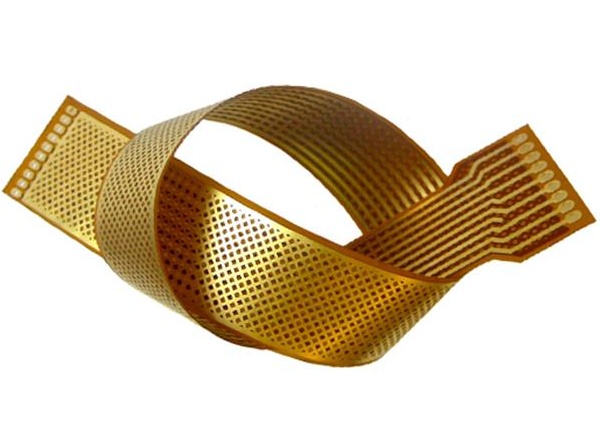
Single sided flex PCB
Single sided flex PCB, with only one layer of conductor, can be covered or uncovered on
the surface. The insulating base material used varies with the application of the
product. Commonly used insulating materials are polyester, polyimide,
polytetrafluoroethylene and soft epoxy-glass cloth.
Single sided flex PCB can be further divided into the following four categories: 1) Single-sided connection without covering layer
The conductor pattern of this kind of single sided flex PCB is on the insulating
substrate, and there is no covering layer on the conductor surface. Like a common single
sided rigid PCB. This kind of product is the cheapest one, usually used in non-critical
and environmentally friendly applications.
The interconnection is realized by soldering, welding or pressure welding. It is often
used in early telephones.
2) One-sided connection with covering layer
Compared with the former class, this class only adds a layer of covering layer on the
conductor surface according to the customer's requirements. When covering, the bonding
pad should be exposed, and it can be simply left uncovered in the end area. If required,
clearance holes can be used. It is one of the most widely used single sided flex PCB,
and is widely used in automobile instruments and electronic instruments.
3) Double-sided connection without covering layer
This kind of connection pad interface can be connected on the front and back of the
wire. For this purpose, a via hole is made in the insulating substrate at the pad, which
can be punched, etched or made by other mechanical methods at the desired position of
the insulating substrate. It is used for mounting components and devices on both sides
and for occasions needing soldering. There is no insulating substrate in the pad area at
the via, and such pad area is usually removed by chemical methods.
4) Two-sided connection with covering layer
This class is different from the former class in that there is a covering layer on the
surface. However, the cover layer has a via hole, which also allows both sides of the
cover layer to be terminated, and still maintains the cover layer. This kind of single
sided flex PCB is made of two layers of insulating materials and one layer of metal
conductor.
It is used in situations where the covering layer needs to be insulated from the
surrounding devices, and itself needs to be insulated from each other, and the front and
back sides of the ends need to be connected.