Global high-mix volume high-speed PCBA manufacturer
9:00 -18:00, Mon. - Fri. (GMT+8)
9:00 -12:00, Sat. (GMT+8)
(Except Chinese public holidays)
Global high-mix volume high-speed PCBA manufacturer
9:00 -18:00, Mon. - Fri. (GMT+8)
9:00 -12:00, Sat. (GMT+8)
(Except Chinese public holidays)
HomePage > Blog > Knowledge Base > Overview of 6-Layer PCB Stack-Up Manufacturing
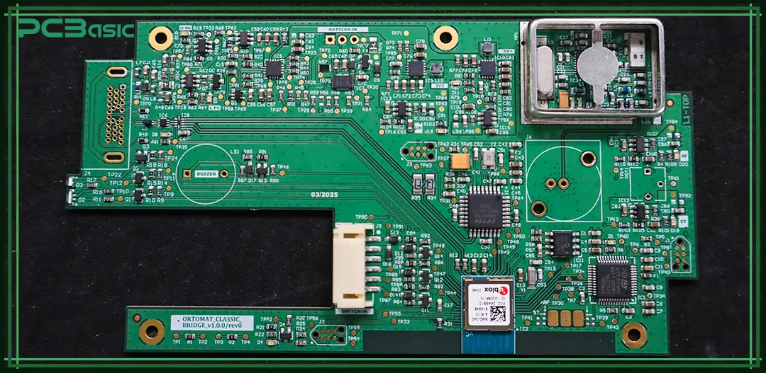
A 6-layer PCB board, as the name states, is a board that contains 6 layers. The typical 6-layer PCB stack-up usually consists of internal planes, signal layers, and power/ground layers. It might sound complicated, but it is often necessary because some complex systems require advanced PCB designs.
The 6 layers of the PCB board are determined based on the application. Some applications will have components that require multiple-layer design while some will have a layout space limitation. This type of limitation prevents a 2 to 4-layer design from being used; 6 layers, however, solve that problem. An additional reason is good signal transmission, which a 6-layer PCB stack-up fulfills.
Different reasons might bring a company or engineer to use a 6-layer PCB board design. Depending on the reason, different techniques and stack-ups should be used during the design process.
Different projects have different requirements. A 6-layer PCB design is considered a complex design that comes with a complicated stack of materials.
Choosing the wrong stack-up could prevent the board from functioning properly. Certain issues could be bad signal output, interference, and the inability of some design features to work. Due to its complexity, it could be difficult to properly debug a 6-layer PCB. Thus, it's important to run all the tests in CAD simulation, which will prevent unexpected issues during the fabrication process.
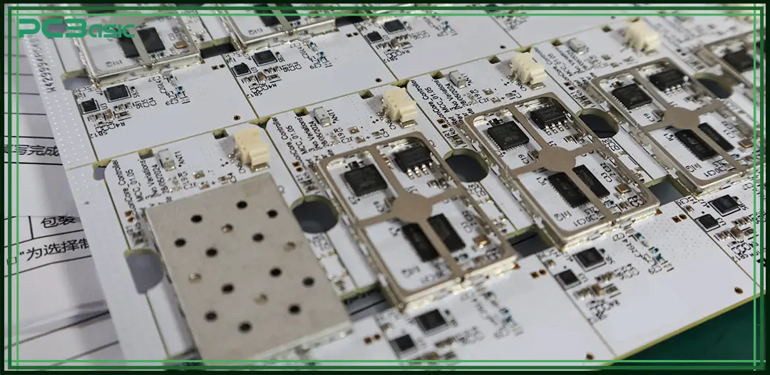
Due to their balanced performance and cost, 6-layer PCBs are widely used in:
• Automotive Electronics – Engine control units (ECUs), ADAS systems
• Telecommunications – Routers, switches, and base stations
• Medical Devices – Imaging systems, patient monitoring equipment
• Industrial Automation – Motor controllers, PLCs
• Consumer Electronics – Smart home devices, high-end audio systems
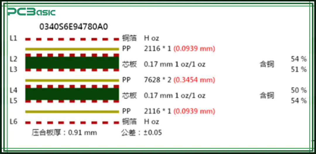
The standard 6-layer PCB stack-up will usually come with the following layers (not in the same particular order):
1. Ground Plane Layer.
2. An Inner Single Layer.
3. Second Inner Single Layer.
4. A Power Plane.
5. A Top Signal Layer.
6. A Bottom Signal Layer.
Although this is the standard and most typical 6-layer PCB stack-up, many other stack-ups exist for multiple reasons. The standard and most typical don’t mean the best one. This kind of decision varies on the application and the use of the 6-layer PCB design.
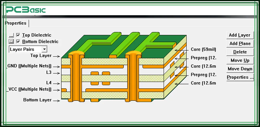
Different PCB designs require different stack-up configurations. It’s important to choose good practice stack-ups that will provide shielding on top of the signal layers. Such shielding will provide good signal transmission and prevent possible faults in the final product. Considering the 6-layer PCB design stack-up before fabrication could save both time and cost.
The most used configuration by engineers will be as follows:
1. A Top Signal Layer.
2. A Ground Plane Layer.
3. An Inner Signal Layer.
4. A Second Inner Signal Layer.
5. A single Power Plane Layer.
6. A Bottom Signal Layer.
These 6 layers will provide good signal transmission and shielding for the signal layers. Additionally, the extra layers of protection could prevent unexpected faults.
The order above isn't perfect and one thing to note is the reduced capacitance due to the separation of the power and ground layers. For that reason, there is another type of 6-layer PCB stack-up to consider that not many people are aware of, such as follows:
1. A Single Top Signal Layer.
2. A Ground Plane Layer.
3. An Inner Signal Layer.
4. A Power Plane Layer.
5. A Single Ground Plane Layer.
6. A Bottom Signal Layer.
We placed the ground and power layers close to each other, in an order that provides better capacitance for the circuit. This was previously considered one of the best 6-layer PCB stack-up practices. However, it’s important to note that each application might contain different requirements. The decision of which layer to stack up to use should be carefully considered.
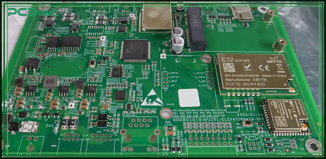
Multiple CAD software can be used to design a 6-layer PCB, the most popular software would be Altium Designer and Eagle, which often customers report as being very useful and easy to use.
Most experienced engineers are able to design a 6-layer PCB, although there is a difference among the final outcomes. Experienced engineers will carefully select 6 layers of PCB stack up to ensure the best compatibility and signal transmission. General knowledge of how to design a 6-layer PCB can be found online. A good design, however, can only be achieved through experience and years of practice.
At PCBasic we have accumulated over 15 years of experience in advanced 2 to 16-layer PCB design. Our expertise is in fields such as aerospace, medical, consumer, and industrial PCB applications.
Whenever your project is in the prototype or mass production stage, we'll provide knowledge and consultation related to your design. A proper 6-layer PCB stack ensures consistency, and compatibility and avoids troublesome and expensive mistakes.
We learned about those mistakes through the years of serving thousands of customers so you wouldn't have to repeat them.
Fabrication of 6 layers of PCBs might sound easy, but it's a complex process; choosing the wrong 6 layers in a PCB fabrication facility could be very costly. When it comes to the PCBA stage and components placement, it's crucial to ensure that the PCBA functions properly and can deliver the proper signal transmission across its designed properties.
For that reason, a quick-turn 6-layer PCB board manufacturing service provides an all-in-one service from PCB to PCBA production that ensures the entire supply chain and production stages go smoothly. By manufacturing the quick-turn 6-layer PCB, we can ensure the board functions properly. Once produced, the board will be delivered to the PCBA factory and verified to be in good condition. This kind of process also eliminates the risk and need of managing multiple suppliers, warehouses, and fulfillment services. If you are worried about your PCB fast turnaround problem, don't hesitate to contact PCBasic!
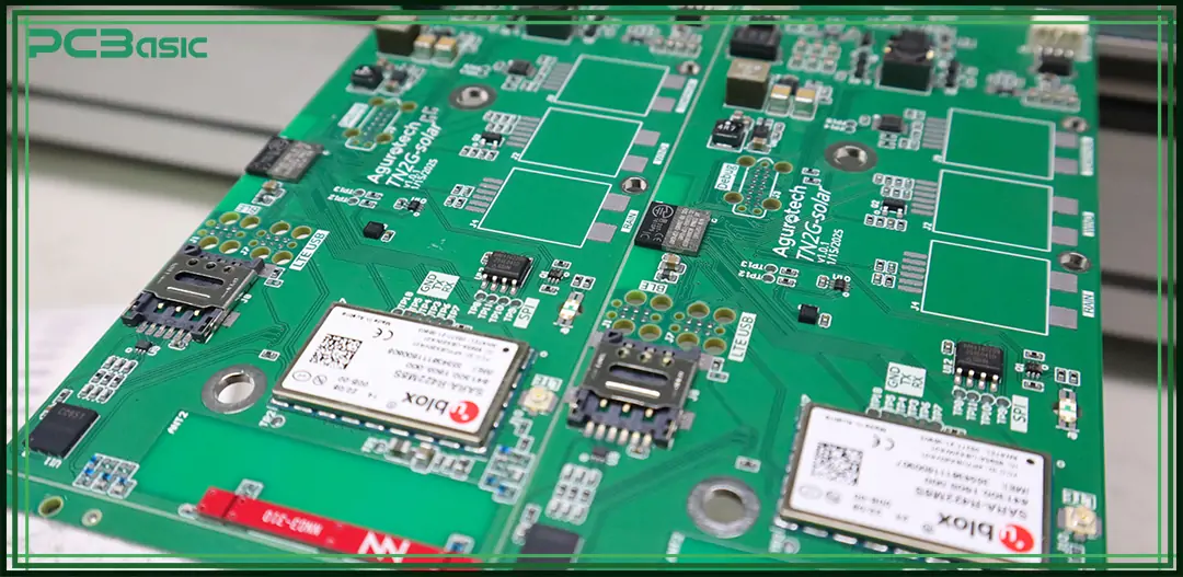
A 6-layer PCB comes with 6 layers that include: internal planes and internal layers, a layer for power and ground, and another two external layers. This kind of stack-up ensures good signal transmission in a complex system.
The materials that PCBs are made of are non-conductive materials, and layers of cooper are both in the internal and the external layers of the 6-layer PCB board. The conductive material in a PCB, commonly known as cooper, is an important material in 6-layer PCB production. Cooper is a highly conductive material that enables us to transmit signals and electricity within the circuit boards.
Depending on the density of the board, the copper layers can go from one or two layers up to 50 layers or even more. Unlike PCBA, producing the PCB board alone eliminates concern regarding the materials, as those are provided and made by the PCB factory itself.
The price for 6-layer PCB prototype can vary, which mostly depends on the quantity of the PCB materials. During the prototyping stage, a cost-effective way will be to produce 5-10 boards at a time. Because of design faults, or for the reason the board hasn’t been tested, ordering a mass quantity might end up going to waste.
Due to the small quantity, the 6-layer PCB prototype price is high. We usually recommend ordering 10 boards instead of 5. This is due to the price and the extra samples that might be needed in the prototyping stage. The price will vary depending on the PCB design size, complexity, and other variables to be determined upon submission to fabrication.
A 6-layer PCB design is not the only design you can choose from. The PCB goes from 2 up to 16 layers or even more, it all depends on the design and application. Most commonly, 4 layers design can be considered for the design of complex applications. Although the designs are quite similar, the 6-layer PCB is more advanced. Often used for applications that require multiple planes with good signal conductivity.
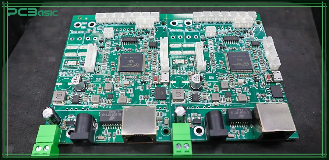
Once we proceed to manufacturing the 6 layers of PCBs, we should note the fabrication facility and the PCBA factory. PCB board production facility shall ensure the ability to produce a good 6-layer PCB. Most of the China PCB factories can do that, although some factories might provide a poorly fabricated PCB. Note that some fabrication facilities and PCBA factories won't usually support a 6-layer design due to the complexity or lack of equipment.
At PCBasic we provide one-stop PCB and PCBA service to fulfill 6 layers of PCB design needs. Our top China PCBA factory serves thousands of customers a year with more than 15 years of accumulated experience.

Assembly Enquiry
Instant Quote
Phone contact

+86-755-27218592
In addition, we've prepared a Help Center. We recommend checking it before reaching out, as your question and its answer may already be clearly explained there.
Wechat Support

In addition, we've prepared a Help Center. We recommend checking it before reaching out, as your question and its answer may already be clearly explained there.
WhatsApp Support

In addition, we've prepared a Help Center. We recommend checking it before reaching out, as your question and its answer may already be clearly explained there.