Global high-mix volume high-speed PCBA manufacturer
9:00 -18:00, Mon. - Fri. (GMT+8)
9:00 -12:00, Sat. (GMT+8)
(Except Chinese public holidays)
Global high-mix volume high-speed PCBA manufacturer
9:00 -18:00, Mon. - Fri. (GMT+8)
9:00 -12:00, Sat. (GMT+8)
(Except Chinese public holidays)
HomePage > Blog > Knowledge Base > The Complete Guide For SMT Process
Nowadays, when it comes to electronic components and equipment, the first word that
comes to mind is associated with circuit boards. Those boards are what we often call
Do you know the difference between these two, and which one is suitable for your PCB
assembly project?
In this article, PCBasic will take you on a journey to understand what is SMT, what
are the specific processes of SMT, and most importantly help you choose the most
There are multiple reasons and benefits implementing SMT in the PCBA fabrication
process:
1. Lead time reduction - compared with traditional plug-in components (DIP
components), the lead time required for through-hole manufacturing is reduced or
sometimes even eliminated. This results in the ability to produce a volume of SMT
electronic products in small components SMD count. The volume of electronic
products processed by SMT chip processing techniques instead of using DIP
techniques can effectively reduce the lead time by 40%~60%.
2. Functionality - High reliability and function, strong anti-vibration ability, not easy to
be affected by vibration which can ultimately cause component failure.
3. Solder paste defects - The defect rate of solder joints during this technique is
considered low, which ultimately improves the placement efficiency.
4. Automation - SMT is an automated process, saving labor, time, and cost during the
placement of the components.
SMT is a multi-stage process that involves multiple stages and complex techniques in
order to be accomplished. eventually, SMT will result in a great PCBA finished product.
Let's walk over the stages to understand what does the standard SMT process looks
like:
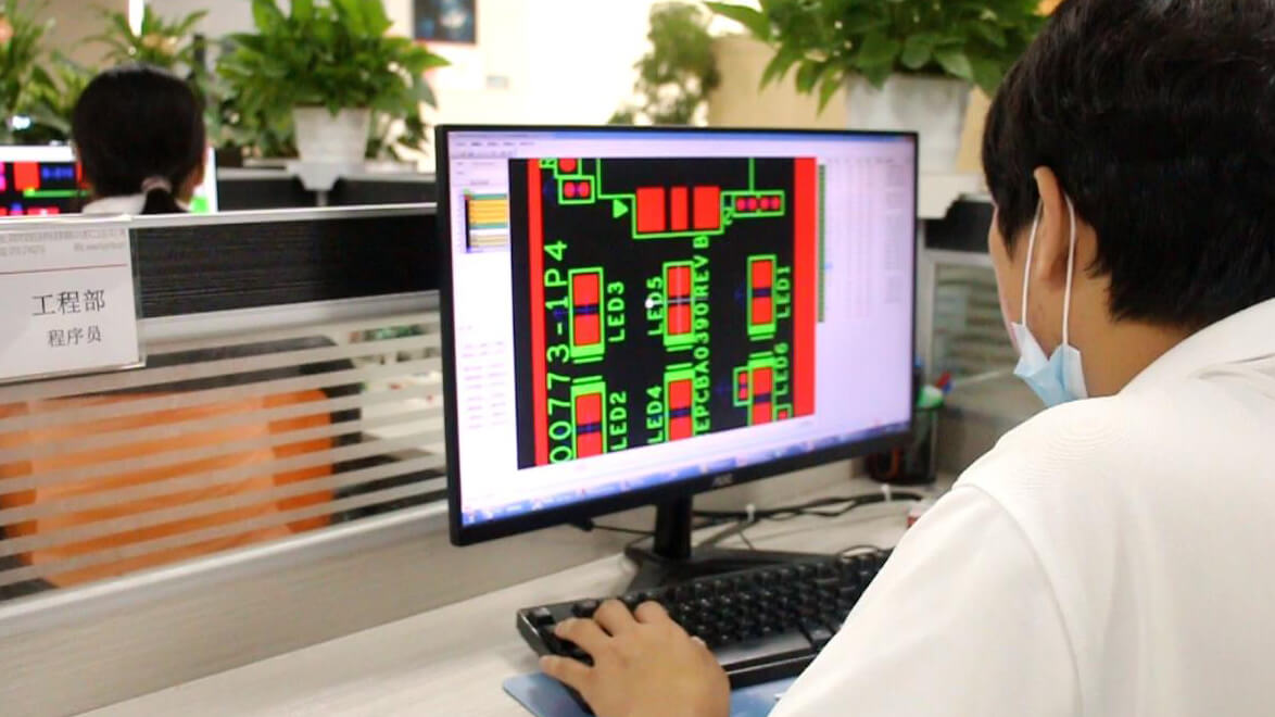
SMD materials (components, integrated circuits, etc… ) are provided by customers or
purchased by SMT manufacturers directly.
After receiving the materials, the warehouse will check the quantity and check the
correctness to check whether the materials are consistent with the pads.
At the same time, The engineer in charge of the SMT process will make the SMT
production program according to the Gerber files and BOM table that was provided by
the customer during the project submission and evaluation process. Once this stage is
complete, the engineer will upload the program files to the corresponding production
line to prepare for production.
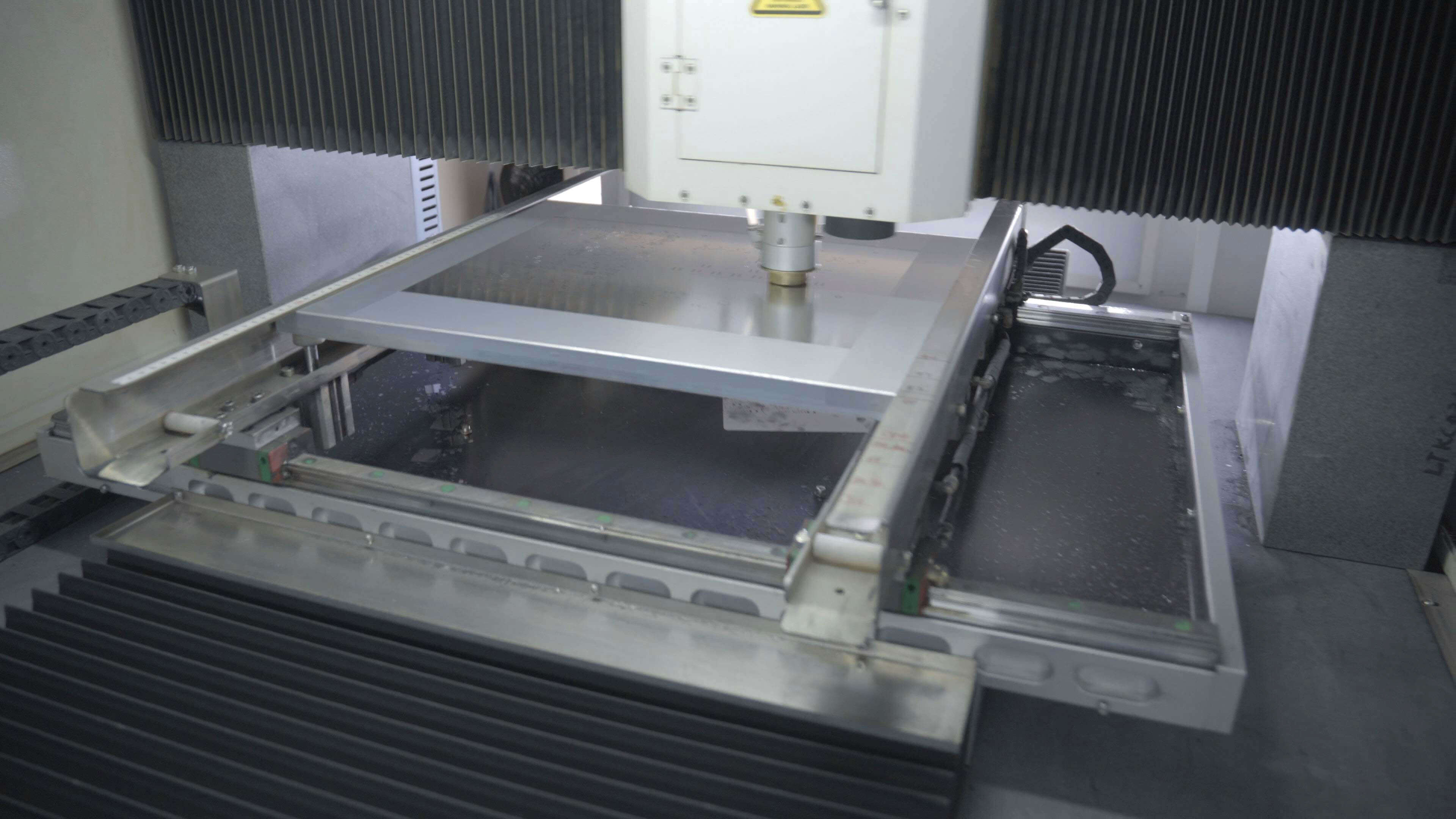
The engineer in charge of the stencil production makes the stencil printing template
according to the PCB pad layer (from the Gerber files provided by the customer). The
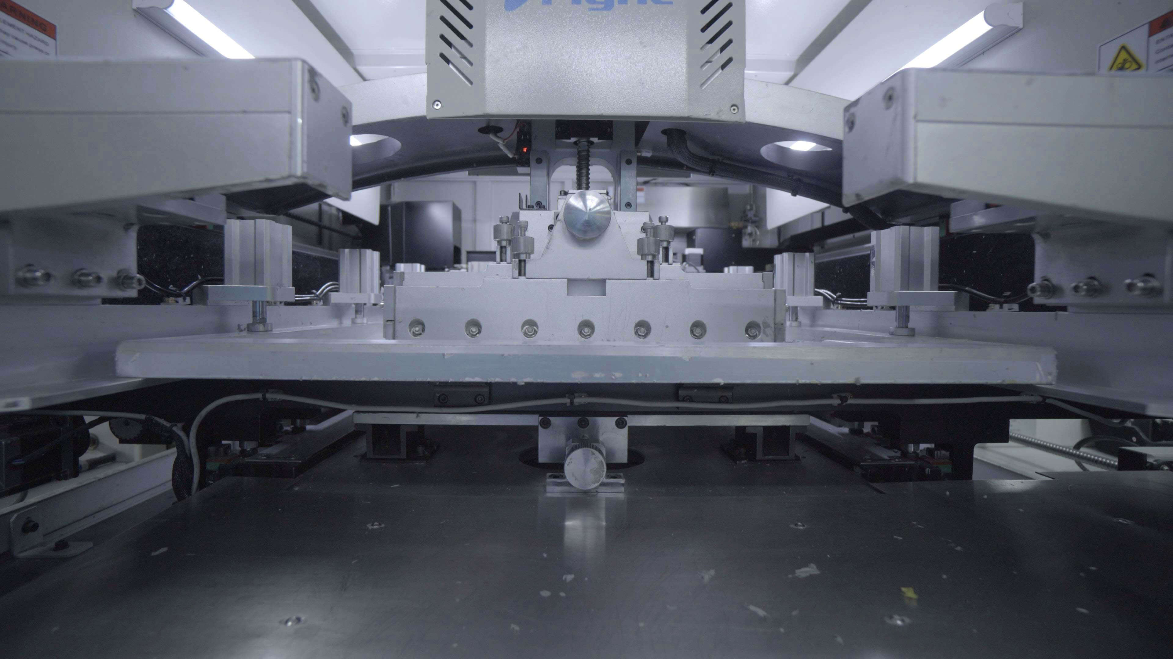
At this stage, The PCB manufacturer and associated engineers will check whether the
stencil is in line with the PCB designs provided by the customer.
The engineers will also check whether the stencil has blocked holes and whether the
solder paste was used correctly. After the inspection, stencil fixes will be applied to the
printing machine and the engineer will run a debug program to ensure the printing
machine operating properly.
During the normal printing process, the operator should regularly check the tin to ensure
that the solder paste doesn’t overflow. If an overflow is detected, the engineer will
collect the overflowing solder paste to ensure the SMT process goes smoothly.
IPQC (process quality control) software will conduct a visual inspection on the first 5-10
sheets printed, and inform the operator whenever to continue the production or stop it if
the printing quality doesn’t match the expected results.
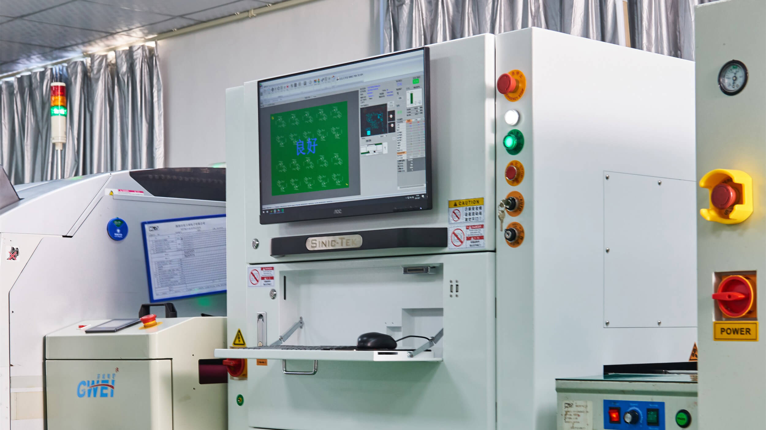
SPI detection designed to test the effect of the solder paste printing. This test will check
whether there are any undesirable results occur in the SMT solder printing process such
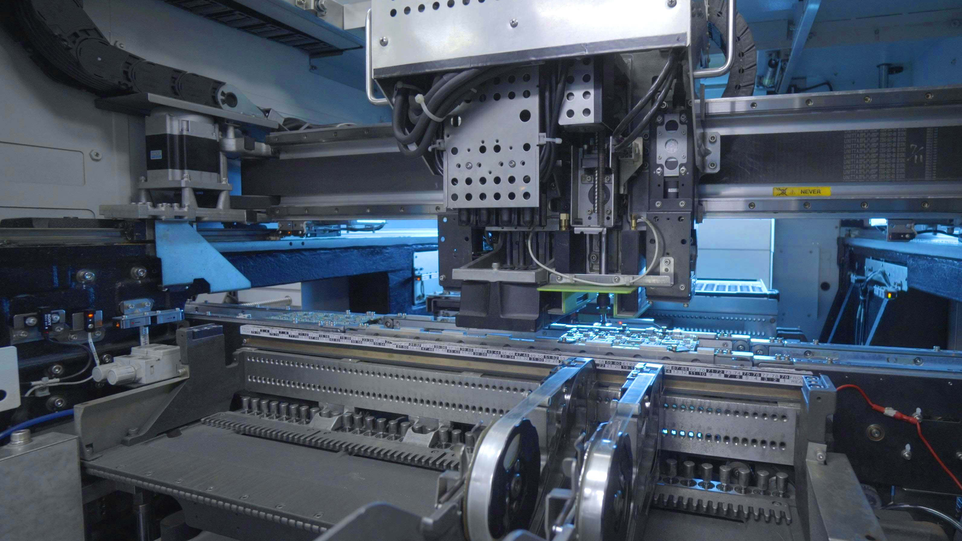
During this stage, the machine will accurately identify the positioning and the placement
of the SMT components. Once the position was accurately configured, the machine will
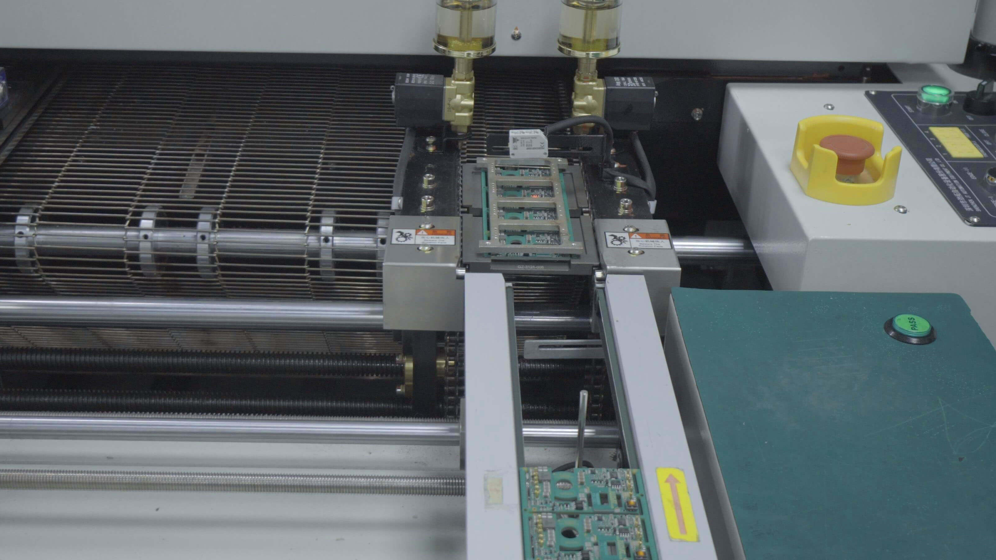
During this stage we monitor the production temperature curve, melt the surface mount
solder paste through the reflow soldering technique and complete the curing process
SMT assemblers and fabrication facilities analyze the changes in the reflow oven
according to the temperature curve of the reflow soldering, this enables them to obtain
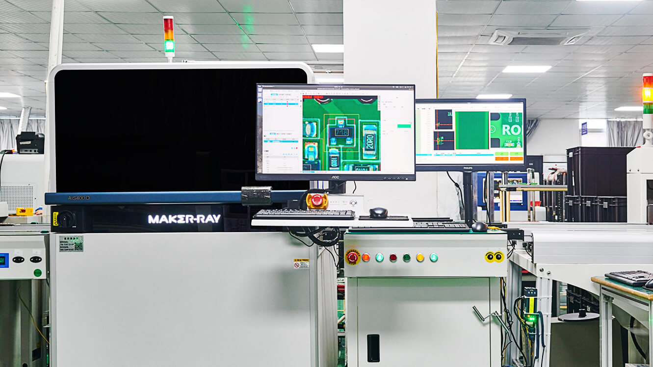
The AOI inspection machine is an automatic optical inspection equipment which scans
the mounted PCBA, collects real-time images and compares them with pre-existing
This kind of advanced machinery powered by AI and computer vision enables SMT
fabrication facilities to make better decisions according to the board state.
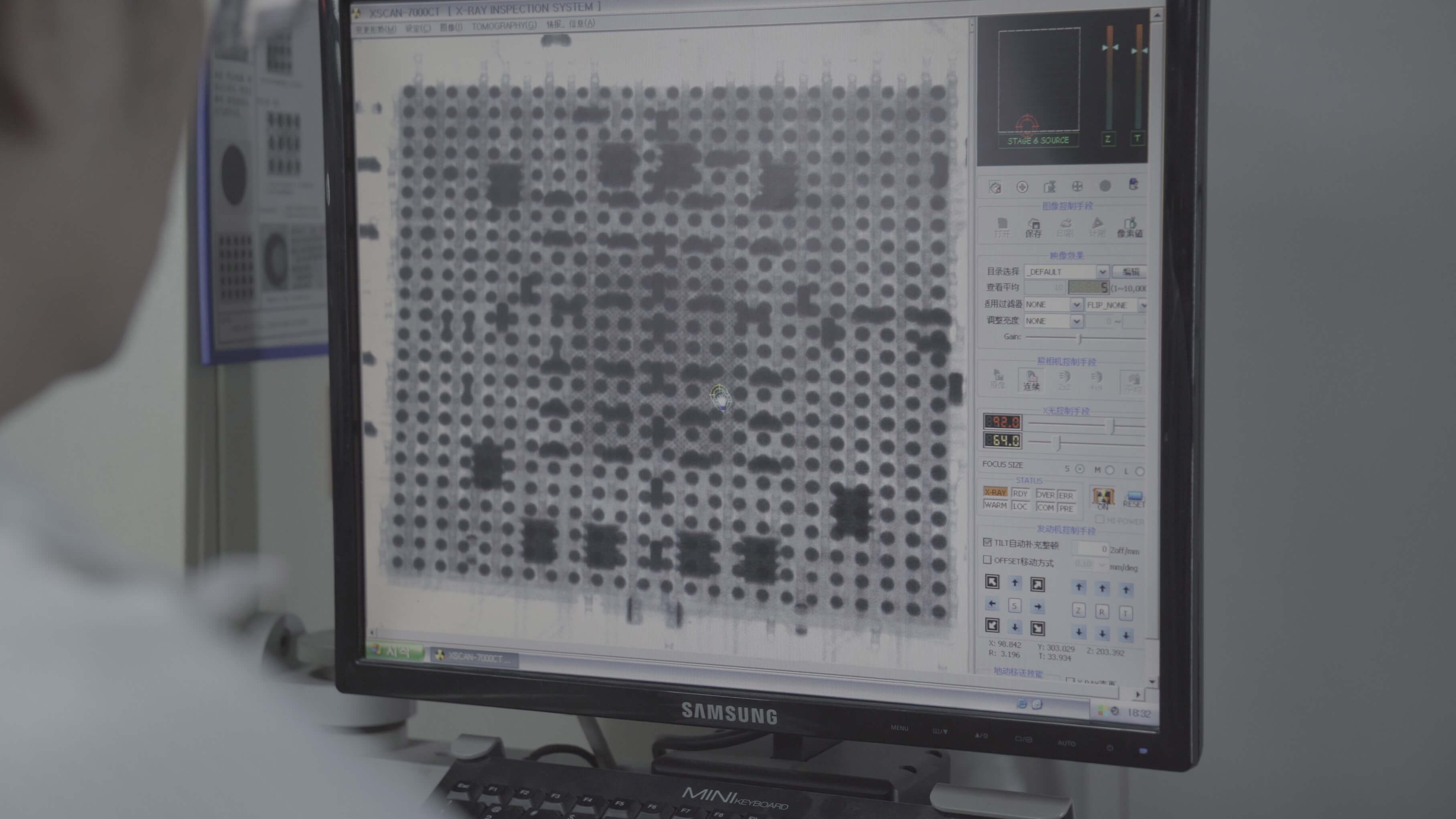
This process applies to some of the SMT lines, particularly those that include BGA (ball
grid array components).
Due to the nature and characteristics of BGA PCB, the soldering state and result
cannot be visually inspected and AOI machines cannot detect the specific details either.
For that reason, it is necessary to use the X-RAY penetration using X-RAY equipment to
detect the electronic components' solder paste state which will help to check, verify and
judge if the SMT solder waste was soldered successfully.
In such situations, timely detection of de-soldering, voids, cold welding, bridging,
displacement, incomplete melting of solder balls, solder beads, and other defects will
drastically improve the quality control of the assembled products.
However, X-Ray inspection equipment is relatively expensive, and many small SMT
assemblers are hesitant to purchase such equipment. This will eventually result in the
inability to effectively detect poor soldering of BGA Assembly.
1. Maintain constant temperature and humidity in the SMT workshop, the specified
temperature is 25±3℃, and the humidity is 65%±5%RH.
2. The use of solder paste should follow the principle of first-in, first-out.
3. When the solder paste is opened and used, it needs to go through two processes of
re-warming and stirring.
4. Ensure electrostatic protection, and control the electrostatic voltage that may be
generated to keep it under a safe threshold for the most sensitive components.
5. Pay attention to the daily maintenance of SMD machines and equipment.
6. Always pay attention to the setting of the process parameters of reflow soldering,
and the furnace temperature must be tested twice a day.
7. In the process of SMT production, it is necessary to use a class of solvents such as
anhydrous ethanol, flux, etc. The SMT production area needs to pay special
attention to fire safety design.
8. Regularly conduct random spot checks on products on the production line, and deal
with abnormalities in time.
Standardized SMT production processes can guarantee high-quality PCBA boards.
Efficient placement is the best way to ensure a speedy project delivery date according
to tight schedules and short lead-time.
Choosing a suitable and professional pcb assembly supplier is the most important
decision to ensure fast delivery of assembled electronic boards and excellent quality of
products.
Follow us at PCBasic, In the next article will explain what DIP is and why and how it
differentiates from SMT explained today.PCBasic is a one-stop PCBA manufacturing
service provider, contact us and we will provide you with the best quality and
consistency for your next PCBA project.

Assembly Enquiry
Instant Quote
Phone contact

+86-755-27218592
In addition, we've prepared a Help Center. We recommend checking it before reaching out, as your question and its answer may already be clearly explained there.
Wechat Support

In addition, we've prepared a Help Center. We recommend checking it before reaching out, as your question and its answer may already be clearly explained there.
WhatsApp Support

In addition, we've prepared a Help Center. We recommend checking it before reaching out, as your question and its answer may already be clearly explained there.