Global high-mix volume high-speed PCBA manufacturer
9:00 -18:00, Mon. - Fri. (GMT+8)
9:00 -12:00, Sat. (GMT+8)
(Except Chinese public holidays)
Global high-mix volume high-speed PCBA manufacturer
9:00 -18:00, Mon. - Fri. (GMT+8)
9:00 -12:00, Sat. (GMT+8)
(Except Chinese public holidays)
HomePage > Blog > Knowledge Base > Ground Plane in PCB Design: Definition, Purpose, and Best Practices
In modern PCB design, if you want your circuits to run smoothly, with stable signals and minimal interference, a very important way is to include a well-designed ground plane. It is like the "foundation" in the circuit board, helping signals get a clear return path and reduce noise.
Whether it is for high-speed digital circuits or radio frequency (RF) products, a reliable PCB ground plane design can greatly improve the performance and reliability of the system.
This article will explain what a ground plane is, what its function is, how it differs from the power plane, and how to create an excellent ground plane design.

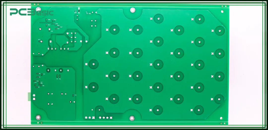
A ground plane refers to a whole copper layer laid on the PCB, whose main function is to provide a stable and low-impedance return path for the current. We can understand it as the "ground" of the circuit board. After all the signals are transmitted, they all need to return through the circuit. This is what people often ask, "what is a ground plane".
The PCB ground plane is usually placed on the inner or top layer of the PCB, which can effectively reduce electromagnetic interference (EMI), avoid ground loops, and stabilize the voltage throughout the circuit. This is particularly important when dealing with high-speed signals and radio frequency (RF) circuits, such as in antenna ground areas.
In PCB design, the ground plane is not only a structural layer but also a key element to ensure the stable performance of the circuit. A well-designed ground plane can enhance the electrical performance of the circuit board in multiple aspects, which are specifically reflected in the following aspects:
Suppressing Electromagnetic Interference (EMI)
A continuous ground plane helps shield the board from external noise sources and reduces the electromagnetic c emissions. By optimizing the ground plane design, the EMC performance of the product can be effectively improved to meet regulatory compliance requirements.
Providing a Low-Impedance Return Path
When high-speed signals are transmitted, the current return needs to flow back to the source. The ground plane provides a current return path with the shortest and lowest impedance for these signals, thereby reducing signal reflection, crosstalk and jitter, and improving signal integrity.
Stabilizing Voltage Reference
The ground plane acts as a common voltage reference for the entire system. It can reduce the errors caused by fluctuations in ground potential and enhance the stability of analog and digital circuits, which is particularly important in multi-power supply or multi-subsystem scenarios.
Supporting RF and High-Speed Signal Applications
In RF design, the ground plane works with signal traces to form microstrip or stripline structures, which are crucial for impedance control and signal shielding. Especially in the antenna ground area, a continuous and complete ground layer is a prerequisite for ensuring RF performance.
Simplifying Routing and Structural Design
Through a reasonable PCB ground plane layout, the routing efficiency of multilayer boards can be improved, the pairing of signals and return paths can be simplified, and the design complexity can be reduced.
 About PCBasic
Time is money in your projects – and PCBasic gets it. PCBasic is a PCB assembly company that delivers fast, flawless results every time. Our comprehensive PCB assembly services include expert engineering support at every step, ensuring top quality in every board. As a leading PCB assembly manufacturer, we provide a one-stop solution that streamlines your supply chain. Partner with our advanced PCB prototype factory for quick turnarounds and superior results you can trust.
According to the differences in the design complexity of the circuit board, signal frequency and performance requirements, the structure of the ground planes will also vary. Common PCB ground plane configurations include the following types:
Single-Layer Ground Plane:
Single-layer ground planes are usually applied in circuit boards with simple structures or low signal frequencies. This kind of ground plane is generally located on the top or bottom layer of the PCB, mainly used to provide a basic return path and minimal anti-interference capability.
Although the single-layer ground layout is relatively simple and has a lower cost, it is prone to problems such as return path interruption and increased EMI in high-speed signals or densely routed designs. Therefore, it is not suitable for designs with high requirements for signal integrity.
Double-Layer Ground Plane
Double-layer ground planes are commonly seen in two-layer PCB designs. It can be placed on the top and bottom sides respectively, providing a more flexible signal routing and better control over high-frequency return currents.
Compared to single-layer ground planes, this type of design is more stable and can better shield noise and reduce signal crosstalk. It is a cost-effective solution between low-end and high-performance.
Multilayer PCB Ground Plane
For high-speed digital, RF or complex multi-chip systems, multilayer ground planes are usually required. This structure distributes the ground plane and power plane in different inner layers to form a stable reference plane, thereby achieving better signal integrity and less electromagnetic emissions.
Multilayer boards can also sandwich high-speed signal traces between two ground plane layers to form microstrip or stripline structures, which greatly enhance impedance control and signal isolation capabilities.

To achieve an efficient and reliable ground plane design, it’s important to pay attention to the following points during PCB layout:
1. Keep the Ground Plane Continuous
The ground plane should be as complete and unbroken as possible. Avoid unnecessary splits, slots, or cuts. If the ground plane is divided, the return path for signals becomes longer and more complicated, which can lead to unstable impedance and increased EMI. In high-speed and RF designs, a continuous PCB ground plane is essential for maintaining signal integrity.
2. Use Vias to Connect Ground Layers
In multilayer PCB designs, the ground planes on different layers should be connected using plenty of ground vias. This helps form a unified, low-impedance return path network, reduces voltage differences between layers, and improves noise immunity.
3. Isolate Noise Sources from Sensitive Signals
High-frequency or high-current components (such as DC/DC converters, inductors, and crystals) should be placed away from analog signal lines or low-noise digital circuits. On the ground plane, these noisy areas should be separated or spaced out from sensitive areas to avoid interference.
4. Place Decoupling Capacitors Close to Power Pins and Connect to Ground
Each chip should have decoupling capacitors placed as close as possible to its power pins. The ground side of the capacitor should be directly connected to the ground plane. This helps quickly suppress high-frequency power noise and prevents it from spreading across the board.
Antenna Ground and Multilayer Design
In RF applications—especially in circuit boards involving wireless communication, BLE, Wi-Fi, or cellular antennas—the integrity of the antenna ground is very important. A multilayer PCB can provide a continuous, solid, and low-noise ground plane under the antenna area, which helps achieve the best possible signal transmission and reception performance.
Therefore, for products that require strong RF performance, using a multilayer PCB ground plane is almost always necessary.
The power plane is a dedicated copper layer in a PCB that delivers power. Unlike signal traces that carry data, the power plane is used to distribute voltage stably, quickly, and with low impedance to every component on the board. Its job is to ensure all parts receive reliable power without voltage drops or interference.
A ground plane is often confused with a power plane, but they serve different functions:
|
Feature |
Ground Plane |
Power Plane |
|
Purpose |
Provides a return path for signals |
Delivers power to components |
|
Signal Reference |
Yes |
No |
|
EMI Control |
High |
Moderate |
|
Typical Use |
All layers, high-speed routing |
Separate planes for VCC, etc. |
Both the ground plane and power plane should be kept solid and carefully planned to avoid noise coupling and ensure stable operation.
A well-designed ground plane is the key to whether a PCB can run stably and resist interference. Whether you're working on analog circuits, digital logic, or wireless RF, as long as you follow proper ground plane design principles, you can achieve cleaner signals, less noise, and more stable system performance.

Assembly Enquiry
Instant Quote
Phone contact

+86-755-27218592
In addition, we've prepared a Help Center. We recommend checking it before reaching out, as your question and its answer may already be clearly explained there.
Wechat Support

In addition, we've prepared a Help Center. We recommend checking it before reaching out, as your question and its answer may already be clearly explained there.
WhatsApp Support

In addition, we've prepared a Help Center. We recommend checking it before reaching out, as your question and its answer may already be clearly explained there.