Global high-mix volume high-speed PCBA manufacturer
9:00 -18:00, Mon. - Fri. (GMT+8)
9:00 -12:00, Sat. (GMT+8)
(Except Chinese public holidays)
Global high-mix volume high-speed PCBA manufacturer
9:00 -18:00, Mon. - Fri. (GMT+8)
9:00 -12:00, Sat. (GMT+8)
(Except Chinese public holidays)
HomePage > Blog > Knowledge Base > What is Wave Soldering? A Complete Guide
In modern electronic manufacturing, soldering is an indispensable process in the assembly of printed circuit boards (PCBs). It determines whether the electrical connections are reliable and also affects the functional stability and service life of the product. Among various types of soldering, wave soldering is one of the earliest technologies to achieve large-scale automated production.
Up to now, wave soldering is still widely used in industrial electronics, power equipment, automotive electronics and other fields. Although reflow soldering has become one of the mainstream processes after the popularization of surface mount technology (SMT), for products that still use through-hole components, wave soldering remains an irreplaceable and important soldering method.
This article will introduce complete wave soldering, from basic concepts to detailed technical processes. We will explain how it works, the soldering machines required, typical application scenarios, main advantages and disadvantages, and compare wave soldering with other common soldering methods. If you are an electronic engineer, product designer, or engaged in PCB manufacturing, this guide will help you fully master wave soldering and improve your production process and product quality.
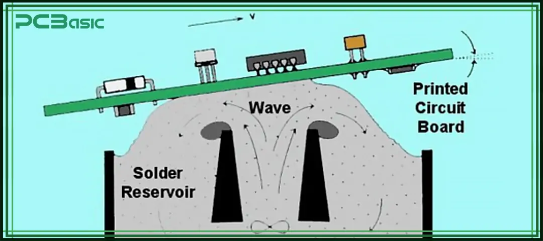
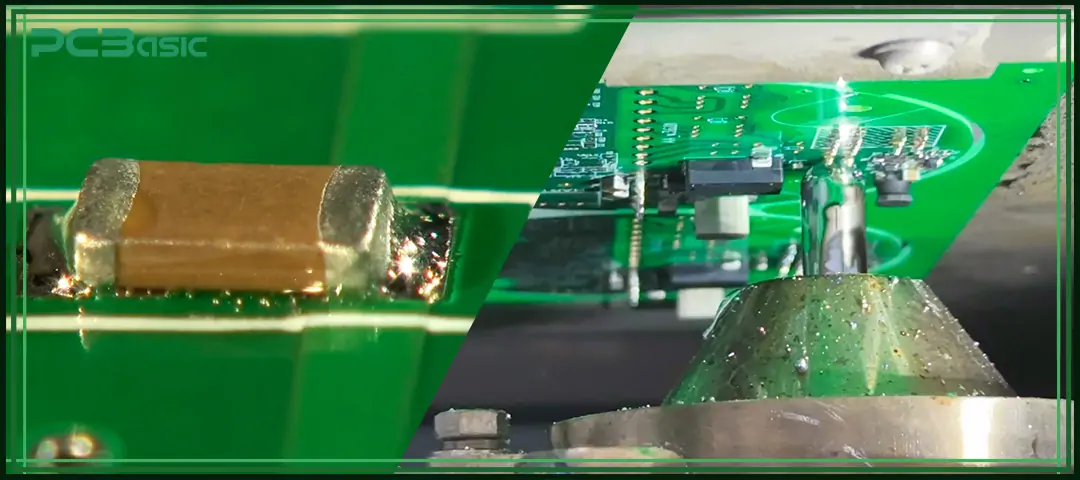
Wave soldering is a soldering technology suitable for mass production. It is mainly used to solder through-hole electronic components onto printed circuit boards. During this process, the assembled PCB passes through a continuous flow of molten solder. The wave solder at the bottom contacts the bottom side of the PCB, forming a strong and electrically conductive solder joint between the component leads and the PCB pads.
This technique is called "wave soldering" because the wave soldering machine it uses, which has a nozzle that pumps molten solder upwards from the solder pot to form a stable solder wave. This wave is the key part of the entire wave soldering process.
Compared with manual soldering, wave soldering is faster, produces more consistent solder points and offers higher reliability. It is a cost-effective and efficient soldering method, especially suitable for large-scale PCB assembly tasks where manual operation cannot meet the requirements of efficiency and consistency. For circuit boards with a large number of through-hole components, it remains an irreplaceable and important soldering method.
Wave soldering is very suitable for the following situations:
• Through-hole components, where the pins pass through the PCB;
• Mixed- technology PCBs (THT + SMT), which can use pallets to protect SMT components;
• Applications that require strong mechanical connections, such as power electronics and automotive systems;
• Demand large-scale production lines with high capacity.
• High-volume production lines that demand high throughput.
Compared with other types of soldering, wave soldering has the following advantages:
• Compared with manual soldering or reflow soldering, it is faster to process through-hole components.
• The solder joints have good consistency and are firm and reliable.
• Reduce labor costs and minimize errors in repetitive assembly.
Although wave soldering has been partially replaced by reflow soldering in the SMT field, it remains an irreplaceable and important process in many industrial applications and scenarios with high reliability requirements.
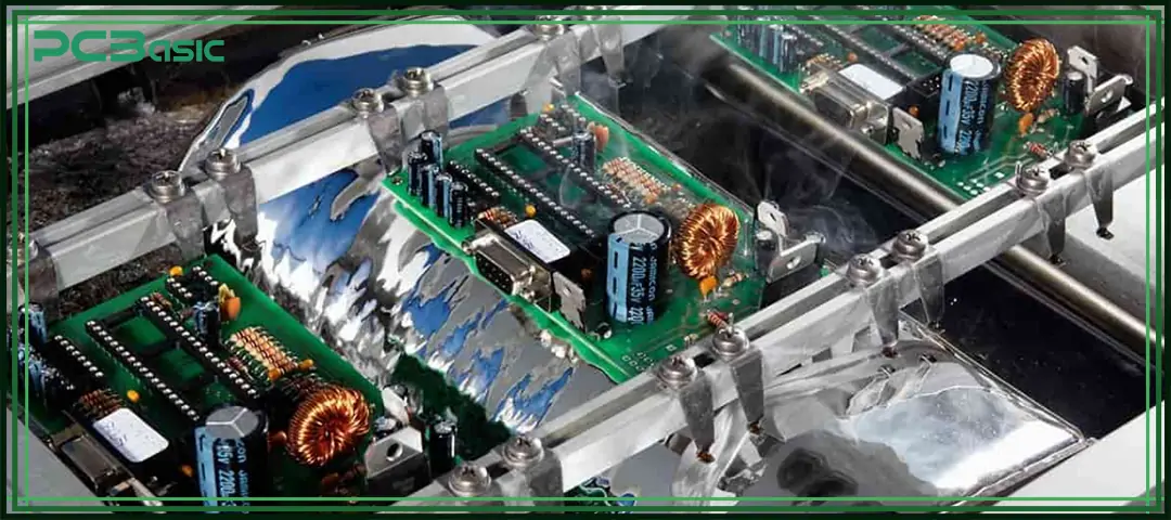
Wave soldering machines are generally classified into single wave, dual wave, and multi-wave (or selective wave soldering) systems, each suited to different assembly needs.
Single-wave soldering uses only one wave of molten solder, which is usually a turbulent wave or a smooth wave. This process is suitable for soldering standard through-hole components and is used for PCBs with simple structures and low circuit density. The equipment is simply designed and has a low cost, making it suitable for producing large quantities of low-complexity products. However, it has poor support for fine-pitch components or double-sided boards and is prone to defects such as missed soldering or bridging.
Double-wave soldering is equipped with two solder waves. The front wave is used to remove flux residue and enhance wetting, while the rear wave is used to form the final solder joint. This setup is suitable for soldering high-density components and PCBs with THT+SMT mixed assembly. Compared with single-wave systems, double-wave soldering has better solder point quality and can effectively reduce the risks of bridging and cold soldering. It is currently the most widely used type of wave soldering.
Multi-wave soldering uses multiple independently controlled solder waves and is mainly used for precise soldering of localized areas. It is often used for THT soldering near the area where SMT components have been mounted, which can prevent thermal damage to the nearby components. This solder method is suitable for products with complex structures or high reliability requirements, but the machine price is high, and the production efficiency is relatively low. It is suitable for small-batch and high-demand occasions.
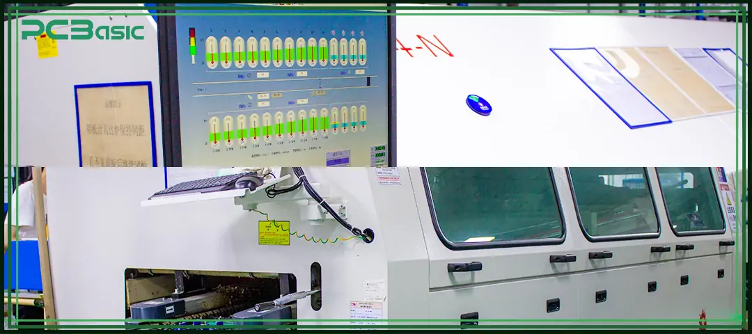
The wave soldering process typically consists of the following steps, each of which directly affects the quality and stability of the soldering.
Before soldering, through-hole components need to be inspected, their leads are trimmed and inserted into the PCB board. If it is a mixed assembly board, SMT components are usually completed first via reflow soldering.
Flux is applied to the bottom of the PCB using spray or foam to remove oxides, enhance wetting and prevent bridging. The amount of flux used should be well controlled. Too much or too little will affect the soldering effect.
Preheating can reduce thermal shock and activate the flux. The temperature is generally controlled between 90 and 125°C and adjusted according to the number of PCB layers and complexity. Heating is commonly carried out using hot air, infrared, or a combination of both.
The underside of the PCB passes over the solder wave, where molten solder forms joints between component leads and pads. Key parameters include solder temperature (approximately 245-255°C), conveyor speed (1-3 cm/s), and dwell time (2-4 seconds).
The cooling rate needs to be controlled after soldering. Cooling too quickly is prone to cracking, while cooling too slowly makes the solder joints brittle. The common methods are forced air cooling or water cooling, and sometimes temperature gradient control is combined to reduce thermal stress.
After soldering is completed, visual inspection, AOI (automatic optical inspection), and functional testing are required. If necessary, X-ray inspection should be carried out to ensure the quality of the solder points.
 About PCBasic
Time is money in your projects – and PCBasic gets it. PCBasic is a PCB assembly company that delivers fast, flawless results every time. Our comprehensive PCB assembly services include expert engineering support at every step, ensuring top quality in every board. As a leading PCB assembly manufacturer, we provide a one-stop solution that streamlines your supply chain. Partner with our advanced PCB prototype factory for quick turnarounds and superior results you can trust.
To ensure defect-free wave soldering, the following parameters must be monitored:
|
Parameter |
Recommended Value |
Purpose |
|
Preheat slope |
≤ 2°C/s |
Prevent delamination |
|
Flux density |
2–5% solids |
Improve wetting, reduce residue |
|
Solder temp |
245–255°C |
Ensure full wetting |
|
Wave height |
5–12 mm (adjustable) |
Adequate contact with leads |
|
Dwell time |
2–4 seconds |
Complete wetting and bonding |
|
Cooling rate |
1–2°C/s |
Avoid warping, improve reliability |
Advanced wave soldering machines allow digital control and logging of these parameters for real-time quality assurance.
• Not ideal for fine-pitch SMT components
• Risk of solder bridging if the setup is poor
• Thermal stress may cause board warping
• Requires large floor space and maintenance
• Flux residue may need post-cleaning
Despite these limitations, wave soldering is still widely used in power equipment, automotive electronics, industrial control and other fields, and is an irreplaceable soldering method in some cases.
Reflow soldering is a widely used soldering method in surface mount technology (SMT) and is very common in the production of modern electronic products.
The basic process of this technology is as follows: First, solder paste is applied to the pads of the PCB using screen printing or similar techniques. Then, components are mounted on the solder paste. Next, the assembled PCB is sent into a dedicated reflow oven. By controlling the heating process, the solder paste gradually melts and the soldering is completed at the appropriate time and temperature, ultimately forming a metal connection between the component pins and the pads.
The entire reflow soldering process is typically divided into four temperature zones:
• Preheat Zone: The PCB is gradually heated after entering the oven to reduce thermal shock and prevent damage to components caused by sudden temperature changes.
• Soak Zone: The temperature is held within a stable range to evenly heat the entire PCB and activate the flux, allowing it to clean and promote solder wetting.
• Reflow Zone: This is the most critical zone. The temperature quickly rises to the solder paste’s melting point, allowing the solder to melt and form solder joints.
• Cooling Zone: After leaving the high-temperature area, the PCB is rapidly cooled to solidify the solder joints and ensure strong and reliable connections.
The main advantages of reflow soldering are high solder joint accuracy, good soldering consistency, suitability for high-density devices, and easy automation of the entire process. This makes reflow soldering the most commonly used soldering method in SMT processes, widely applied in the manufacturing of various products such as consumer electronics, communication equipment, and computer hardware.
|
Feature |
Wave Soldering |
Reflow Soldering |
|
Component type |
Through-hole (THT) |
Surface-mount (SMT) |
|
Heat source |
Molten solder contact |
Hot air / infrared oven |
|
Temperature |
245–260°C |
220–250°C (peak) |
|
Speed |
Faster for THT |
Slower but more precise for SMT |
|
Suitable for |
High current / mechanical strength |
High-density, compact devices |
|
Cost |
Lower for bulk THT boards |
Higher for setup and materials |
|
Defect risks |
Bridging, residues |
Tombstoning, solder balls |
Types of soldering are often combined: SMT components reflow-soldered on one side, then wave soldering for THT on the other.
Wave soldering is a mature and reliable soldering method, suitable for soldering through-hole components onto printed circuit boards. Although many products now use reflow soldering, wave soldering still has obvious advantages in mass production, high mechanical strength requirements, or high-reliability fields such as industry and automobiles, especially in terms of high speed and low cost.
As long as the appropriate wave soldering machines are equipped, the key process parameters are reasonably set, and the role of each step is understood, manufacturers can achieve stable and high-quality soldering results. Whether it is building a new production line or improving the existing process, mastering wave soldering technology is a key stage to ensure efficient and reliable PCB assembly.
Assembly Enquiry
Instant Quote
Phone contact

+86-755-27218592
In addition, we've prepared a Help Center. We recommend checking it before reaching out, as your question and its answer may already be clearly explained there.
Wechat Support

In addition, we've prepared a Help Center. We recommend checking it before reaching out, as your question and its answer may already be clearly explained there.
WhatsApp Support

In addition, we've prepared a Help Center. We recommend checking it before reaching out, as your question and its answer may already be clearly explained there.