Introduction
Every product must undergo testing before it is finally sent to the shelves for customers. Similar is the case with PCBs; the printed circuit board is one of the major components of most of the electronics we have around us used regularly; hence, there is no room for negligence.
PCB testing is one of the main stages that has to be taken care of during the manufacturing process of PCBs. The main reason to conduct this kind of printed circuit board testing is to ensure that there are no defects in the PCB, and this way, the task of covering the PCB quality inspection is also carried out.
The discussion on PCB testing is a detailed one. There are so many vital things to know, and if you are also interested in learning about the significance of the PCB test and how to test the PCB board, you are at the right place.
The guide below covers all the essential information on the PCB testing methods, so let's read below.

Benefits of PCB Testing
Most manufacturers consider printed circuit board testing an essential part of the PCB manufacturing process because of its ample benefits. Some of these benefits are discussed below:
Helps Identify Issues
One of the significant benefits of PCB testing is that it helps identify problems. Some issues may lie in manufacturing a PCB, and some may lie in functionality. It is essential to test the board to determine where the issue lies and whether or not the PCB is functional.
The printed circuit board testing helps identify the defects in the design and layout of the PCB so that it can be altered as needed.
Helps Save Time
When the PCB testing is carried out in the initial stages, which could be the prototyping stage, the further steps become easier to flow with. Identifying the issues in PCB design and functionality at the start will help the designers and manufacturers fix them immediately.
Timely adjustments ensure fast production and reduce the lead time of making them reach the market.
Reduces the Cost
Ensuring timely PCB testing minimizes waste in the form of defective products. In cases where the faults are identified later, there is a high chance that the entire stock of the assembled products will go in vain. Hence, this causes a lot of waste of resources as well as money.
Timely initial testing helps fix the issue immediately, and then further processing occurs, free from defects. Moreover, the cost of production also decreases.
Low Rate of Returned Products
Companies that ensure a timely inspection and conduct PCB tests are on the safe side when they float the PCB boards in the market. The defects are addressed timely, and there is no need to have any replacements demanded.
Therefore, PCB testing helps reduce the return rate of the products from the market, which is always a hassle for the manufacturer and an added cost.
Helps Address Safety Concerns
PCBs are used widely in most electronic equipment. Hence, their performance must be up to the mark. When PCBs fail, this may lead to a fire hazard that harms the users.
Hence, when PCBs are appropriately tested, the chance of such hazards is reduced, and the safety concerns are adequately addressed.

What Should Be Tested During PCB Manufacturing?
Testing PCB at the manufacturing stage is very important. It helps to fix the issues right away and saves time and costs. Once the PCB is ready and faults are found, resolving them becomes troublesome. Some of the essential aspects that need sufficient testing are as follows:
Quality of Lamination
Lamination of the PCB is very important; once the PCB is laminated, it becomes a hassle to peel that lamination. Therefore, it is suggested to assess the quality of it at the stage of manufacturing. A good quality lamination doesn't come off due to force or heat, and this is what needs to be tested.
Quality of Copper Plating
It is essential to test the quality of the copper that is being played on the PCB plays a significant role. Copper offers conductivity to the board, but if the quality of the copper is compromised, there is a high chance that the strength of the PCB will be compromised.
Quality of Solder Material
The functionality of PCB depends on the firmness of the components attached to the board. Hence, the solderability of the material is very important for the components to be firm enough and for the PCB to perform efficiently. Therefore, analyzing how perfectly the surface reacts to the solder is essential.
Quality of Hole Wall
How a PCB will react to thermal stress and drastic temperature changes is very important to consider. Hence, when it comes to testing a PCB at the manufacturing stage, it must be checked for hole-wall quality. The hole wall must not crack when subjected to thermal stress and pressure during manufacturing.
Electrical Conductivity
A PCB is used in electrical devices; hence, it must pass the electrical currents with as little leakage as possible. Therefore, it is essential to test the electrical conductivity of the PCB when testing it at the manufacturing stage.
Environmental Resistance
PCBs are subjected to different kinds of environments; sometimes, these environments may be humid, and hence, they should be capable of passing the water absorption test to ensure it doesn't fail when subjected to moisture.
Similarly, corrosion is a common issue that must be avoided for better functionality of PCB. Hence, it should be tested for corrosion even by putting it to different environmental conditions.
Common PCB Testing Methods
If you are thinking of PCB testing methods, below, you will find numerous ways to help you with a PCB test.
1. In-Circuit Testing (ICT)
In-circuit testing is one of the most opted PCB testing processes, which most PCB manufacturers choose. This method tends to identify more than 90 percent of the defects because it offers varied PCB testing tools.
In the process of in-circuit testing, there is a PCB tester, which comprises a matrix having sensors and drivers in the count of hundreds and thousands, and they conduct the test measurements.
The in-circuit tester also contains a PCB test fixture, which directly interacts with the tested PCB. The PCB test fixture comprises nails connected to the points on the board, and they gather the information from the board and transmit it to the fixture.
It also comprises a PCB testing software instructing the system to perform relevant tests. It measures the information against the parameters, determining whether the board has any issues.
Pros of In-circuit Testing
● The in-circuit testing method offers testing of individual components.
● It helps in measuring capacitance, resistance, and multiple other measures.
● It helps test the PCB at the final stage and supports testing high-volume PCBs.
Cons of In-circuit Testing
● It is a costly testing method.
● It cannot be considered for early-stage testing.
● In-circuit testing is not suitable where the testing volume is low.
Applications:
The in-circuit testing method is ideally suitable for analog circuits, and in these circuits, it helps in measuring the capacitance, resistance, and various other analog measures.
2. Flying Probe Testing (FPT)
")
Flying probe testing is a method for PCB testing, also known as fixtureless in-circuit testing. It was first invested in 1986, and since then, it has been able to offer PCB testing without custom fixtures.
The flying probe testing method uses fixtures that hold the PCB; the testing pins move around the board and keep testing the board. A PCB testing software controls these pins, which detects the issues through this movement.
Pros of Flying Probe Testing
● Flying probe testing can adapt to new boards in no time.
● It is a very convenient method of testing PCBs.
● This technique of testing PCB is far more affordable than other methods.
Cons of Flying Probe Testing
● The testing process is slow.
● It is suitable for low volume due to lack of speed and hence not for high volume testing.
Applications:
Flying probe testing is a suitable method for checking a PCB board, which is complex and low volume. It goes well for removing and repairing the PCB and carries out agile testing.
3. Automated Optical Inspection (AOI)
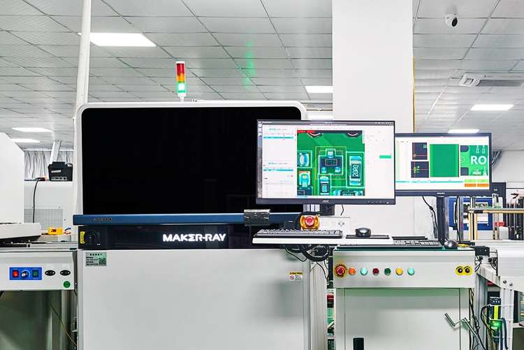
Automated optical inspection is a contactless PCB testing method. It uses microscopes and cameras to perform the testing.
In automated optical inspection, microscopes and cameras are used where they take pictures of the PCB. Then, the software used for testing PCB looks for defects and inconsistencies in the board. Every board is inspected in detail visually, and the issues are spotted immediately to resolve them.
Pros of AOI
● This testing method can be used at all stages of PCB manufacturing, even after the PCB is manufactured.
● It finds defects in the board and the components on the PCB.
● AOI is the best option to identify issues with the connections on PCB.
Cons of AOI
● AOI doesn't cover all the types of PCB board parts; hence, it needs to be combined with the other testing methods.
● It doesn't identify the non-visible defects on the board.
● It doesn't detect the functional defects.
Applications:
Automated optical inspection is applied to detect defects, inspect solder, verify components, inspect leads, inspect through-hole components, etc.
4. Burn-In Testing
Burn-in testing helps to identify the early errors in PCBs and also helps in the analysis of load capacity.
During burn-in testing, the PCB is subjected to thermal and electrical testing. At the start, electricity is applied to the board for over 40 hours. By applying this much electricity, the performance of PCB at high temperatures can be examined.
Moreover, the PCBs are also subjected to pressure and stress to assess their ability to handle environmental tests. In the stress test, these boards are even kept in a burn-in oven for a couple of hours under a specific voltage, and when the test is finished, the board is removed to examine the flaws.
Pros
● Burn-in testing is a PCB testing method that helps identify early PCB failures.
● This method improves the reliability of the PCB and the components present on it by identifying the weaker components.
● Stress testing ensures the strength of PCB.
Cons
● Burn-in testing is expensive as it needs specialized equipment.
● It leads to waste and consumes a lot of energy because of the prolonged burn-in periods.
● Burn-in testing may not help detect every kind of issue.
Applications:
The burn-in testing method for PCB is widely used in medical equipment, data centers, defense systems, and consumer electronics.
5. X-Ray Inspection
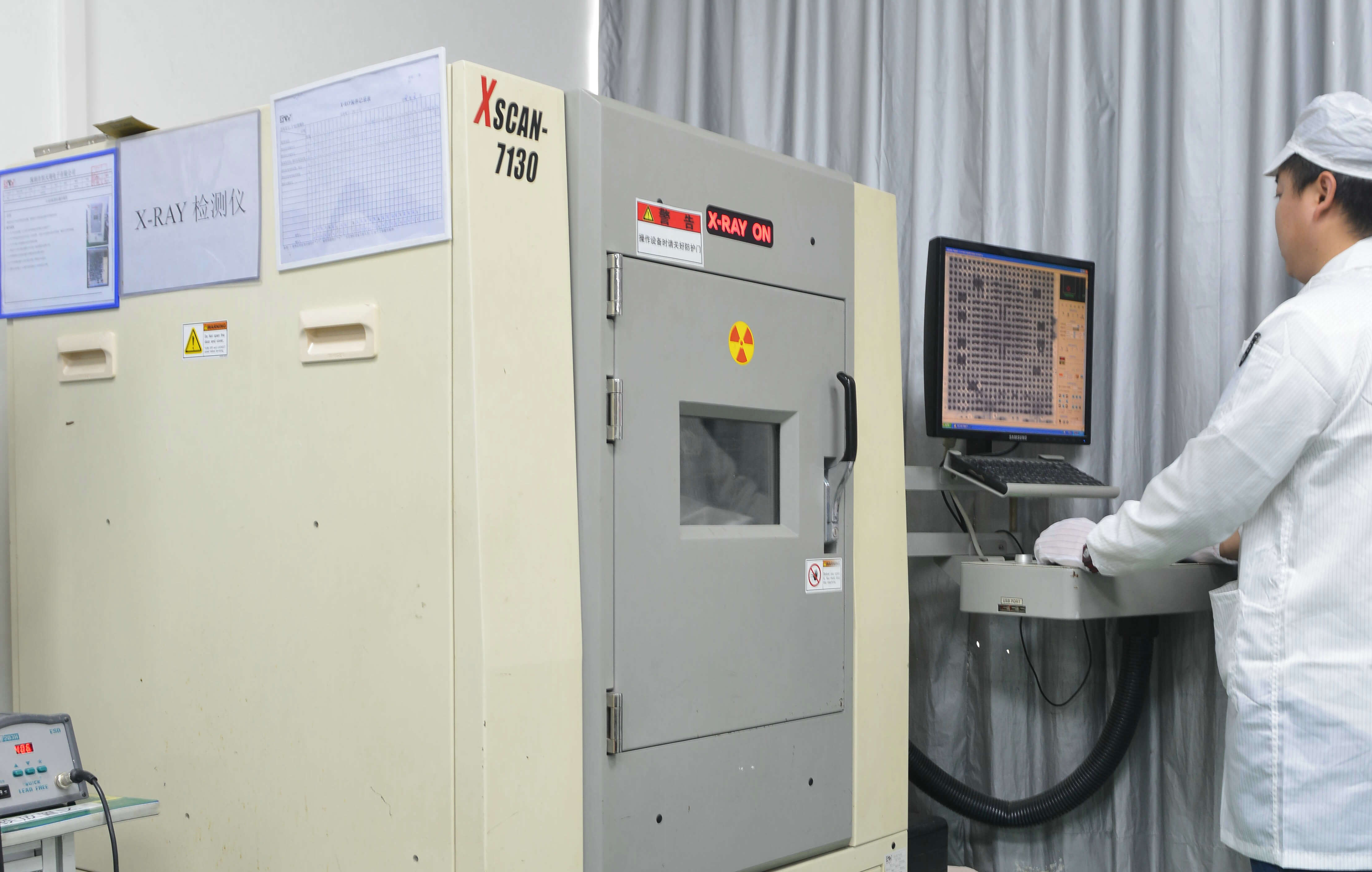
X-ray inspection, as the name suggests, is a testing method for PCBs that uses X-rays to detect defects in the printed circuit board that occur during the manufacturing stage.
During x-ray inspection, solder connections, barrels, and internal traces are scrutinized, which is how the early flaws are detected. The x-ray inspection process generates x-rays, penetrates them into PCB, and carries out attenuation, and once the issues are detected, an image is formed. In this way, we can ensure all components are well soldered and aligned with the PCB board joints. If a component would not solder properly, a manual correction need require to ensure the component’s functionality by pcb functional test system.
The denser components on a PCB can absorb more X-rays than the ones that are not dense, and the back of the PCB is a detector that keeps on capturing the X-rays after transmission.
Pros
● X-ray inspection allows the PCB to carry out the internal examination, and they do this without causing damage to the components.
● This method gives a detailed insight into the defects by providing high-resolution images.
● X-ray inspection is capable of detecting hidden defects, which also include misalignment in the components.
● X-ray inspection offers versatility, which means different materials used for PCB may comfortably be inspected through this process.
Cons
● X-ray inspection equipment used in PCB testing is expensive; maintenance also adds to the cost apart from purchasing it.
● The X-ray causes radiation; hence, it is a concern that these rotations may cause trouble for the surroundings in which they operate.
● Trained and experienced professionals can use this equipment, so the staff needs to be trained before allowing them to operate it.
Applications:
The PCB testing process is used widely in the automobile and aviation industry, electronic and semiconductor industry, and many more to detect the defects in PCBs used for assembling the parts of different products.
6. Boundary Scan Testing
Boundary testing is a PCB testing method that inspects the wire lines, and it is ideally suitable to test integrated circuits as it reaches all the nodes in the circuit.
The process of boundary scan testing moves around a Test Access Port Controller known as TAP. The TAP chooses the operations performed to detect the issues and forms a serial shift register, which shifts the test data through the pins in and out.
At the time of testing, the data and test patterns are loaded on the shift register. It allows the testing and functional behaviors of the integrated circuits to be examined.
Pros
● It is a comprehensive testing process that goes through every detail of the PCB, and apart from detecting the faults, it also assesses the functional behavior.
● This method does not require physical access to the components; hence, densely populated PCBs may be tested without concern.
● Boundary scan testing is a method that can test the PCBs at an early manufacturing stage, hence determining the faults on time.
● It is a cost-effective testing method and works well for high-volume production.
Cons
● The process of boundary scan testing itself is complex; hence, it needs a detailed setup.
● Boundary scan testing is suitable for interconnect testing, but when it comes to determining analog faults, this process is limited to detecting them.
● The boundary scan testing is not functional and only focuses on interconnects.
Applications:
Boundary scan testing is suitable for testing PCBs at the manufacturing stage and also helps verify connectivity in the PCBs.
7. Functional Testing

Functional testing is a PCB test that helps verify the circuits and components of the PCB.
Testing a PCB through functional testing starts with planning, and test cases are developed depending on the strategy devised. It is usually conducted based on the behaviors of the PCB, which are defined and expected and are therefore tested.
PCB receives input signals during the process, and the equipment monitors its response; this helps detect faults.
Pros
● This testing process helps ensure the system meets the end user's requirements.
● This test assesses the system entirely and covers every end-to-end process.
● If there is any system bug or inconsistency, this method helps detect it very efficiently.
Cons
● Functional testing has some limitations like it does not verify the performance, scalability, and load handling of non-functional aspects of a PCB.
● It only covers some scenarios, as testing is only based on the given inputs.
Applications:
Functional testing helps to verify the power distribution and functionality of the circuit and components and looks at the overall system integration.
8. Other Functional Testing
Apart from the suggested testing methods, some other functional tests also help assess a PCB. These tests are as follows:
8.1 Test for Solderability
The solderability test helps to check whether the component on the PCB offers sufficient wetting that leads to creating a more robust connection. It is imperative to carry out this test before completing the assembly process.
8.2 Test for Contamination
Contamination testing carries out the detection of residues that are left behind on the PCB during the process of manufacturing or soldering. It helps to ensure that before a final coating is applied on the PCB, it is clean and all kinds of contamination has been removed.
8.3 Analysis of Micro-Sectioning
It is one of the most essential PCB testing tools, which helps to analyze the failure and also carries out the in-process verification. It checks the internal making of the PCB so that any kinds of open defects or failures can be identified and addressed.
Looking for a PCB or PCBA quote? Contact us now.
How to Test a PCB that Stops Working?
Sometimes, a perfectly working PCB ends up causing technical issues, and in such cases, these PCBs stop working. There are different ways you can test such a PCB, and these are as follows:
Visual Inspection

In a situation where a PCB stops working suddenly, you may need to spot the fault, and for this, you can conduct a visual inspection of the board. You have to look for faulty components, broken traces, and burnt areas, if any.
Focus on the input/output ports' power supply and look at the ICs that are cracked. These defects could easily be detected by conducting a visual inspection.
Power Module Inspection
After visually inspecting the board to see if the components are working fine, you must inspect the power module. You will need to measure the power rail voltage with a multimeter.
Pay attention to the future if the input voltage shows 0 V on the voltage regulator. It usually represents a short circuit, leading to damaging and heating up components.
The overheated components must be removed carefully, and once again, the voltage needs to be checked to ensure no other problem persists.
Input/Output Port Inspection
The input/output ports are also common failure points; when these parts are damaged, they short the entire circuit down and cause abnormality in the entire system. If you have protected the input/output ports using fuses, you must ensure they work well.
Communication Port Inspection
Circuit boards having communication ports like ethernet are also at a high failure risk. In such cases, when a failure is detected. The ICs are checked for burns and cracks, and the protective components are assessed.
How to Protect PCB with Better Designs?
Protection of PCB is essential, so you need to look forward to better designs. Different design techniques are available these days, and opting for them allows you to have better designs that help with PCB protection. Some of these methods are as follows:
1. Design for Manufacturing
Design For Manufacturing (DFM) is a process in which the PCB layout is created and designed in a way that helps to mitigate defects. The main intention of this kind of layout of PCB is to avoid the issues that usually occur during the fabrication and the assembling process.
The PCB layer has some pieces of copper that float freely, and they have a chance to cause issues with the PCB design. They may cause interference, and hence, they should be avoided.
Moreover, the pins and traces with less gap in between also lead to having no solder mask, which creates bridges between the pins and leads to corrosion.
By implementing the design for manufacturing tests, these issues could be avoided, thus protecting the PCB board.
2. Design for Assembly (DFA)
The PCB assembly process requires the attachment of components on the circuits to be carried out very securely. However, in complex design cases, the component attachment may need help.
Design for assembly helps to design PCBs so that assembling becomes simple and quick. The DFA process consists of minimizing the input of material, choosing readily available components, ensuring sufficient spacing between components, and marking the position of components clearly.
3. Design for Test (DFT)
Design for Test helps make the testing process of PCB convenient and affordable. These designs are created to locate defects quickly. Hence, the amount of time spent on testing is cut down while saving the testing cost.
4. Design for Supply Chain
The lifecycle of components on the PCB is also an important consideration; if the components are obsolete, sourcing them becomes difficult. Hence, it is essential to consider designing products with the idea of supply chain and availability of components in the long run.
When designing PCBs, keeping in touch with the suppliers or having alternative solutions is an important consideration.
FAQs About Testing a PCB Board
1). How Do You Test A PCB with A Multimeter?
The probes on the multimeter must be touched on the testing points to test the printed circuit board.
2). How to Test a PCB for Faults?
There are different methods to check a PCB board, including x-ray inspection, in-circuit testing, functional testing, and many more. The PCB can also be visually inspected for any defects.
3). How are PCBs Electrically Tested?
PCBs can be tested electrically once they are manufactured. These boards are tested with the help of a flying probe.
4). What are Common PCB Defects?
The most common PCB defects are gaps in plating, inadequate soldering, lack of copper-to-edge clearance, acid traps, components having defects, etc.
PCB Failure:
|
Physical damage
|
Component failure
|
Manufacturing errors
|
Design flaws
|
Troubleshooting PCBs:
|
Cleaning
|
Visual inspection
|
Electrical testing
|
|
PCB Repair Services:
|
Experience
|
Equipment
|
Supply lines
|
Customer service
|
Common Pcb Problems:
|
Starved thermals
|
Acid traps
|
Silvers
|
Via in Pads
|


