Global high-mix volume high-speed PCBA manufacturer
9:00 -18:00, Mon. - Fri. (GMT+8)
9:00 -12:00, Sat. (GMT+8)
(Except Chinese public holidays)
Global high-mix volume high-speed PCBA manufacturer
9:00 -18:00, Mon. - Fri. (GMT+8)
9:00 -12:00, Sat. (GMT+8)
(Except Chinese public holidays)
HomePage > Blog > Knowledge Base > PCB Drilling: Techniques, Types, and Best Practices
PCB drilling is a key step in the manufacturing of printed circuit boards. Its main function is to create mounting holes for electronic components (such as resistors, capacitors, chips, etc.) and to establish electrical connections between different circuit layers. As electronic products become smaller and more complex in function, higher requirements have been put forward for the accuracy and stability of circuit board drilling.
This article will introduce the basic principles, types of drilling, common techniques, technological processes, design precautions, quality inspection methods and solutions to common problems of PCB drilling. Whether you are a beginner or an experienced engineer, this guide can help you better understand and apply the drill for PCB.
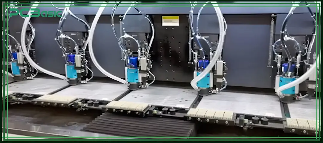
PCB drilling refers to the process of drilling various types of holes on printed circuit boards (PCBs) for installing electronic components or connecting conductive paths between circuit layers. These holes are usually drilled by mechanical drilling or laser drilling, and special tools are used to drill the PCB.
Whether it is a simple single-sided board or a complex high-density multilayer board, circuit board drilling has a direct impact on the performance and reliability of PCBs. Common types of drill holes include plated through holes, non-plated through holes and vias.
In high-speed or radio frequency (RF) circuits, unused via stubs can affect signal quality. At this point, the backdrilling or back drill PCB technology can be adopted to remove excess copper from the other side of the PCB to reduce interference and improve signal integrity.
During the process of PCB drilling, various types of holes are generated according to different functional requirements. Each type of hole plays a different role in the circuit board, and its size and positional accuracy must be strictly controlled during design and manufacturing.
The plated through-hole is drilled completely through the PCB. After the drilling is completed, a layer of copper will be electroplated on the hole wall. The copper layer enables electrical connections between different layers. This type of hole is widely used for installing pin-through-hole components such as resistors and capacitors, and can also serve as part of via conduction connection.

Non-plated through holes are drilled without electroplating. They have no electrical conductivity and are mainly used in mechanical structures, such as screw fixing holes, alignment or through holes for assembly. These holes are only used for physical support or structural alignment.
Vias are used for electrical connections inside multilayer circuit boards. According to different connection positions, they can be further classified into the following types:

• Through-Hole Vias: Drill from the top layer to the bottom layer, connecting all layers.
• Blind Vias: Drill from the surface into one or more inner layers without penetrating the entire board.
• Buried Vias: Located entirely within the inner layers of the PCB, connecting internal layers only and not visible on the outer surfaces.
• Microvias: Extremely small vias, typically with a diameter under 150 μm. Commonly used in high-density interconnect (HDI) designs and created using laser drilling.
• Thermal Vias: Designed to dissipate heat from high-power components. The copper-plated hole conducts heat from the component's surface to the inner or bottom copper layers.
Each type of hole needs to be processed using the appropriate PCB drilling techniques. For instance, mechanical drilling is suitable for most PTHs and NPTHs, while micro-holes require laser drilling. All drilling must comply with the PCB design requirements and meet strict tolerance and positioning requirements to ensure the electrical performance and reliability of the final product.
For different design complexities, types of materials and specifications of holes, PCB drilling can adopt various technical methods:
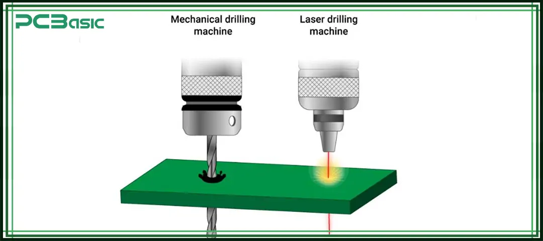
Mechanical drilling is currently the most common and mature technology in PCB drilling. It uses high-speed rotating carbide drill bits (such as tungsten steel) to create holes in PCB materials. This method is applicable to the majority of plated through-holes (PTH) and vias used for electrical connections. Because mechanical drill bits have good processing strength and durability, they are very suitable for high-volume, consistent drill PCB production
In modern circuit board drilling production lines, CNC (Computer Numerical Control) drilling machines are one of the core equipment. l. These machines are controlled by programmed instructions that direct the drill head's movement and cutting path, delivering high precision in terms of hole diameter, position, and depth. CNC machines can meet the tight tolerance requirements of high-density and multilayer PCBs.
Laser drilling is an advanced, non-contact PCB drilling technique primarily used for producing microvias, especially in HDI (High-Density Interconnect) circuit boards. A high-energy laser beam is focused on melting and vaporizing the substrate material, enabling extremely fine holes with diameters typically smaller than 150μm—much finer than what mechanical drilling can achieve.
Mill machine drilling is a more traditional drill PCB method that involves manual or semi-automatic control. It offers flexibility in the machining process and is often used for prototyping, small-batch production, or R&D purposes. Operators manually position the drill based on the PCB layout, which, although less efficient and precise than CNC equipment, is practical for design verification and short-run manufacturing.
 About PCBasic
Time is money in your projects – and PCBasic gets it. PCBasic is a PCB assembly company that delivers fast, flawless results every time. Our comprehensive PCB assembly services include expert engineering support at every step, ensuring top quality in every board. As a leading PCB assembly manufacturer, we provide a one-stop solution that streamlines your supply chain. Partner with our advanced PCB prototype factory for quick turnarounds and superior results you can trust.
|
Method |
Description |
Application Scope |
Advantages |
Disadvantages |
|
Mechanical Drilling |
Uses high-speed rotating carbide bits for standard drilling |
Through-holes, vias, mass production |
Mature, low-cost, widely used |
Larger holes, not suitable for microvias |
|
CNC Drilling |
Computer-controlled drilling with automatic tool changes |
Multilayer PCBs, HDI, fine-pitch designs |
High precision, efficient, multi-board capable |
Expensive equipment, complex maintenance |
|
Laser Drilling |
Uses laser beams to vaporize material for tiny holes |
Microvias, HDI, high-speed applications |
Ultra-precise, non-contact, minimal stress |
High cost, slower for large holes |
|
Milling Machine |
Manual or semi-automatic drilling for prototypes or small runs |
R&D, prototyping, low-volume jobs |
Flexible, low cost, easy to operate |
Low efficiency, limited accuracy |
Below is a standard circuit board drilling process, covering each step from alignment to cleaning. This ensures the accuracy and quality of PCB drilling in production.
Before drilling, location holes are created on the PCB panel. These act as registration points to ensure proper alignment of multilayer PCBs and prevent layer misalignment. For high-layer-count PCBs, X-ray PCB drilling is often used. It helps align the outer layer drilling with inner layer patterns to ensure drilling accuracy for mass production.
Before actual drilling, the PCB panels are stacked with an aluminum entry sheet on top and a back-up board at the bottom. The entry sheet helps with heat dissipation and prevents drill bit deflection, while the back-up board reduces burrs at the drill exit. The stack is fixed with tape and alignment pins to prevent movement during the drill PCB process, ensuring drilling precision.
After setup, CNC drilling machines or manual tools drill the holes. The drill path is generated by CAD/CAM engineers and exported as NC Drill or Excellon files. The machine drills holes based on this data. Common holes include plated through holes (PTH), non-plated through holes (NPTH), and vias. Each hole type uses specific drill bits and parameters according to the design. This is one of the most critical steps in PCB production, directly affecting connectivity and component placement.
After drilling, a first-article inspection is done to ensure results meet design requirements. This includes checking for hole position accuracy, correct hole diameter, burrs, or resin smear. This step helps detect early process errors and prevent batch defects. Some manufacturers also use Automated Optical Inspection (AOI) to check drilling quality.
The final step after PCB drilling is cleaning and burr removal. A brushing machine is commonly used to remove mechanical burrs. Plasma cleaning or compressed air can also be used to remove dust and debris. This step improves plating and soldering quality and ensures no contaminants affect the final product. It is essential for making reliable PCBs.
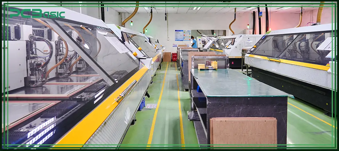
To ensure high-quality circuit board drilling, several key design and manufacturing factors must be considered. These factors help keep the PCB drilling process stable, precise, and compatible with downstream processes.
Aspect ratio is the ratio of hole depth to hole diameter. For standard plated through-holes (PTH), the aspect ratio can go up to 10:1. For microvias, which are usually made by laser drilling, the ratio is about 0.75:1. Designers must keep the aspect ratio within process limits. If the ratio is too high, it may lead to poor copper plating inside the hole or blocked holes.
The annular ring is the copper pad area surrounding a drilled hole. If the ring is too narrow, small drill misalignment can cause a breakout (pad breakout), resulting in weak solder joints or failed electrical connections. It's important to make the pad large enough to handle drilling tolerances and ensure solder reliability.
This is the minimum spacing between the edge of the hole and nearby copper traces. If the hole is too close to a trace, drilling the PCB may cause shorts, dielectric breakdown, or signal interference. Following minimum spacing rules reduces risk and improves electrical reliability.
The size and position of the holes must follow strict tolerance requirements. For PTH, the typical hole diameter tolerance is ±3 mil. For NPTH, it's ±2 mil. Via location tolerance is even tighter, around ±1 mil. Keeping these tolerances under control ensures holes fit well with the plating, soldering, and assembly processes. It also prevents dimensional errors that could affect board performance.
By optimizing all these parameters, manufacturers can achieve clean, accurate PCB drilling, maintain proper hole alignment and wall quality, and improve both the electrical and mechanical reliability of the board.
Backdrilling or back drill PCB is a special PCB drilling method used to remove unused parts of vias, called via stubs. This process is important in high-speed and high-frequency circuits because it helps improve signal quality.
Backdrilling removes via stubs that can cause signal reflections. It helps improve impedance matching and reduces issues like deterministic jitter and insertion loss. These benefits are critical in applications where signal transmission must be clean and stable.
First, the via is drilled and plated like a normal through-hole. Then, from the opposite side of the board, a larger drill bit is used to drill down to a controlled depth. This removes the unused part of the via while keeping the electrical connection between the required layers.
Backdrilling is commonly used in telecom equipment, servers, and RF PCBs. In these applications, keeping signal integrity is very important, and backdrilling is an effective solution.
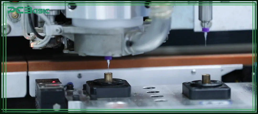
High-quality PCB drilling is ensured through multiple levels of inspection and validation:
Visual and AOI Inspection
• Checks for hole position, size, and cleanliness
Microscopic Inspection
• Detects internal defects or burrs invisible to the naked eye
Cross-Section Analysis
• Reveals plating quality, wall roughness, and annular ring integrity
Electrical Testing
• Validates conductivity between layers post-drill PCB and plating
Drilling Validation Checklist
• Confirm hole count and size match design
• Differentiate PTH from NPTH
• Check for holes < 7 mil (avoid if possible)
• Verify that backdrilling is applied correctly to specified vias
In electronics manufacturing, PCB drilling is a key process that directly affects how well a circuit board works. It’s not just a basic step — it plays a big role in the board’s reliability and performance.
From standard through-holes to more advanced methods like backdrilling, understanding how circuit board drilling works helps engineers make better, more reliable PCBs. If you're working with HDI boards, trying to improve signal quality with back drill PCB techniques, or just aiming for accurate holes, it's important to choose the right drill for the PCB method and follow strict quality checks.
Simply put, whenever you drill PCB, accuracy matters — and it all starts with a good hole.
Assembly Enquiry
Instant Quote
Phone contact

+86-755-27218592
In addition, we've prepared a Help Center. We recommend checking it before reaching out, as your question and its answer may already be clearly explained there.
Wechat Support

In addition, we've prepared a Help Center. We recommend checking it before reaching out, as your question and its answer may already be clearly explained there.
WhatsApp Support

In addition, we've prepared a Help Center. We recommend checking it before reaching out, as your question and its answer may already be clearly explained there.