As you know, PCBs are the backbone of many electronic devices. However, printed circuit boards need protection from delamination. Usually, PCB delamination happens due to manufacturing faults. It's a potentially harmful condition during the manufacturing process and usually results from humidity. Humidity substantially damages the adhesive material and separates the base layers.
Well, a small delamination is bearable but the large scale is what causes real trouble. This article will thoroughly analyze PCB delamination, how to prevent it, and why it happens. So, read it carefully till the end to learn everything about it. Let's get going!
What is PCB Delamination?
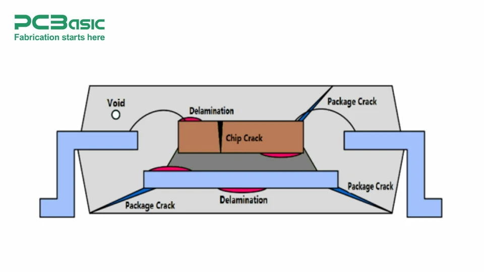
During PCB delamination, the layers of base materials begin to separate from each other. Since PCBs are composed of multiple layers including insulating substrate layers and conductive copper layers. When these layers begin to separate, it weakens the PCB and makes it more susceptible to failure.
Related forms of delamination are also known as PCB measling and PCB crazing. PCB measling is the formation of very small delaminated white spots. While, crazing is a condition when the fibers in the glass cloth and resin material of a PCB separate.
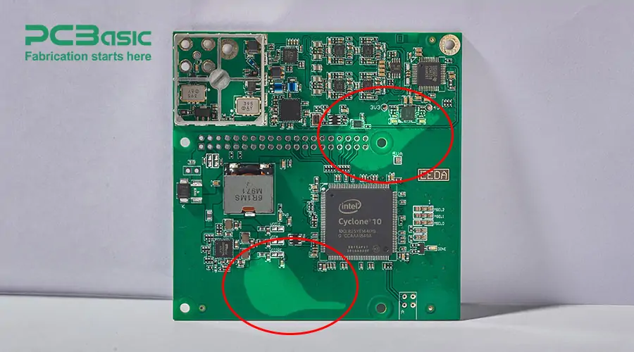
The following example illustrates the delamination on the surface layer of a PCB. The circular discolored area is where the top layers of material are starting to separate from the base material.
What Causes PCB Delamination During Production?
Do you want to know what causes delamination? The following are the main factors that can lead to delamination.
Excess Moisture
The most common reason for delamination is the moisture trapped in the PCB base materials. The unfavorable storage conditions of laminate materials can lead to an uptake in humidity. And, excess humidity in the PCB substrate can cause delamination during fabrication. Furthermore, PCB base materials are hygroscopic. So, they can easily absorb water. Excess moisture in the printed circuit board doesn't always cause delamination, but it'll contribute to CAF (conductive anodic filamentation).
Thermal Stress
The other common factor is the period at which a board is help at high temperatures. Repeated thermal stress can up to high temperatures can cause delamination during assembly. Even after assembly, if the PCB undergoes repeated thermal stress above it's glass transition temperature, the delamination can occur. Delamination due to thermal stress might start in the internal layers without impacting the external layers.
Poor Manufacturing Processes
Poor manufacturing processes can also lead to PCB delamination. PCB has to go through a series of steps during manufacturing such as etching, printing, and plating. If all these steps are completely taken care of, and high-quality materials and equipment are used, there is a significant reduction in the delamination.
Low-Quality Materials
The most significant factor of PCB delamination is the use of low-quality materials. When the quality of materials used in your PCB is not up to the mark, the chances of delamination are higher. Moreover, the use of proper handling techniques for the PCB materials also reduces the delamination process significantly.
Incorrect Type of FR-4 Tg Materials
If you are using FR-4 material with the incorrect type of Tg, than you may face delamination. It can also cause problems with their longevity and reliability. So, it's important to use the correct type of FR-4 Tg materials when manufacturing PCBs. Because, it can affect how well your PCBs hold up over time.
Effects and Consequences of PCB Delamination
Delamination can impact the optimal performance of the printed circuit boards. Its effects and consequences are:
Electrical Performance Issues
Delamination can peel the copper traces from the dielectric. As a result, it can cause crosstalk, signal reflections, impedance variations, and noise that downgrade the board's electrical performance.
High Risk of Failure
Delamination can weaken the PCB's physical structure, making it vulnerable to mechanical stress and mechanical issues.
Reduced Lifespan
Heat issues, weakened structure, and electrical problems reduce the PCB's lifespan and reliability.
Heat Dissipation Problems
Air is not a good conductor of heat as other board materials. And, delamination creates air gaps that develop regions with thermal resistance that can stress active components on the board.
PCB Delamination vs Measling
As I've discussed earlier in this blog post, delamination is the separation of layers of your PCB base materials, which creates bubbles or gaps that look like blisters. This happens in the manufacturing process when humidity or heat are present in your PCB.
On the other hand, PCB measling is the disintegration of pieces in the weaves inside of the board. It can be tolerable and minor until it's not frequent or if it doesn't bridge soldering eyes and conductors. Furthermore, stress during manufacturing process might cause measling.
How to Prevent PCB Delamination?
Following are some tips to avoid PCB delamination.
Keep a Dry Environment
As mentioned above, delamination occurs when the board is exposed to humidity or moisture. So, if you're storing your PCB for a long time, then make sure to keep it dry. The best way is to keep the board in an enclosed container with no cracks or holes.
Proper Baking
Baking of board before thermal processing is a common practice in the PCB industry. This is required because humidity can be trapped between the dielectric and copper layers and cause delamination. Baking of boards before thermal processing helps to eliminate moisture from the board surface. Thus, it'll help to prevent delamination of PCB.
Use High-Quality Components
As mentioned above, the quality of materials and components can impact the performance of the PCB. So, if you make sure to use the high quality materials and components than you PCB will work properly and you'll prevent it's delamination.
Proper Handling
Another common factor to prevent delamination is proper handling. It starts with choosing a supplier that can pass all qualification tests and can meet your needs. Adding more, must store your PCB at optimal conditions that'll not impact it's performance.
Delamination Repair Steps
You can implement delamination repair steps. But, first you need ball mills, cutting tools, a microscope, a micro drill system, syringes, an oven, circuit bond epoxy, and wipes. These repair steps are:
First of all, clean the board's surface by using wipes.
Drill at least two holes into the delamination blister by using the micro drill. Don't drill too deep to expose the circuits or inner planes.
Bake the PCB in the oven to eliminate any moisture if present.
Then, pour the epoxy into the cartridge and inject it into one of the drilled holes.
Apply light pressure on the board if the blister isn't filled properly.
Cure the epoxy at room temperature for 24 hours or at 74°C (165°F) for one hour.
Scrape off any excess epoxy by using a knife or scraper.
Evaluation
After drying, must do a visual examination to check the color and texture. Additionally, do electrical tests on conductors around the repaired areas to see if everything works properly.
Types of Tests to Measure PCB Delamination
There are many tests that can be used to measure delamination. Some of these are:
Scanning Acoustic Microscopy (SAM)
SAM uses ultrasound waves to check the thickness of the materials. This method is specifically useful for delamination when two bonded surfaces separate. Scanning Acoustic Microscopy uses a laser to examine the surface of the material. The laser creates a map of the surface of the material, enabling researchers to assess whether there are any delamination defects or cracks.
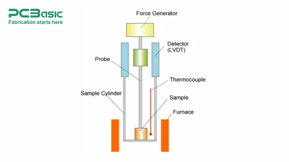
Thermomechanical Analysis (TMA)
This test measures how much energy is required to break a sample. It applies pressure to the sample and then measures how much energy is utilized to break it. If there's no delamination present, then it shouldn't reveal any changes in braking force.
Stress Testing Parameters
It is very important to have clear parameters to get an accurate PCB to withstand periods of high demand. Following are the stress testing parameters to avoid PCB delamination.
Solder Float Test
It's a stress testing parameter and an accelerated lifetime test. It simulates the effects of a solder joint subjected to thermal cycling. This test is performed at 288°C.
Interconnect Stress Test (IST)
This test allow engineers to pull out common modes and thereby reduce problems. This test allows to identify if the PCBs are at risk and that too prior to manufacture. In this test, a static force is applied to the PCB. The static force is applied for ten seconds and then released for 30 seconds. This cycle is repeated for one minute.

N Passes in Reflow Simulation
This test involves stimulating the high-temperature reflow process by heating up and cooling down the PCB multiple times. Each time the PCB is heated up and cooled down is referred to as "N-pass". the number of N-passes in which you can observe no delamination is your max allowable number of N-passes.
Time at 260°C
Do you want to make sure that your PCB will not delaminate? Then make sure that the time at 260°C is greater than ten minutes. Furthermore, the time of temperature of the PCB during testing depends on the type of epoxy used in it's manufacture. Few epoxies are more heat resistant that others. So, they require less time at a high temperature.
Conclusion
To conclude, delamination can occur anywhere. However, substandard manufacturing processes are the main reason behind PCB delamination. Although there are certain techniques to fix the issue, it's better to avoid its occurrence. So, if you need reliable, delamination-resistant PCBs, contact PCBasic right away for high-quality boards customized to your specific needs. Contact us now, and we'll provide you with the boards with minimum to no chance of getting delaminated. Hopefully, we've described all aspects of PCB delamination.