Global high-mix volume high-speed PCBA manufacturer
9:00 -18:00, Mon. - Fri. (GMT+8)
9:00 -12:00, Sat. (GMT+8)
(Except Chinese public holidays)
Global high-mix volume high-speed PCBA manufacturer
9:00 -18:00, Mon. - Fri. (GMT+8)
9:00 -12:00, Sat. (GMT+8)
(Except Chinese public holidays)
HomePage > Blog > Knowledge Base > LM358 Pinout | A Comprehensive Guide
The LM358 is a versatile and widely used dual operational amplifier (op-amp) integrated circuit (IC), suitable for a variety of analog signal processing applications. Operating with a single power supply, it simplifies many designs and is often found in sensor circuits, audio applications, and signal conditioning. The IC consists of two independent, high-gain, internally frequency-compensated op-amps that make it ideal for low-power applications, especially in systems requiring amplification of signals from light-sensitive components like photo diodes, photo transistors, and light-dependent resistors (LDRs).

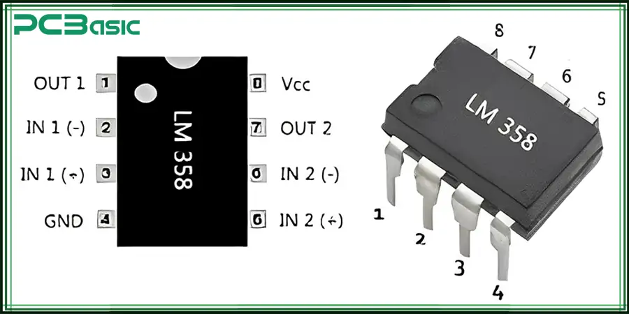
The LM358 comes in an 8-pin dual in-line package (DIP). Each pin has a specific function crucial to the operation of the IC. Understanding the LM358 pinout is essential for designing circuits efficiently and troubleshooting issues in applications such as sensor circuits, where signal amplification is required.
The LM358 operational amplifier offers a variety of package types to meet different PCB design requirements. Among them, the most common packaging types are:
DIP-8 (Dual in-line Package) : This type is suitable for breadboard construction and prototyping.
SOIC-8 (Small Form Factor Integrated Circuit Package) : Suitable for surface mount PCB design.
TSSOP-8 (Thin small form Factor Package) : Suitable for compact and high-density board layout.
Usually, LM358P refers to the DIP package version, and LM358N is commonly found in the DIP-8 package. For surface mount SOIC or TSSOP packages, the pin arrangement of the LM358 SMD Pinout is consistent with that of the DIP version.
When designing or repairing circuits, be sure to refer to the LM358 datasheet pinout *to ensure that the pin connections are correct (the chip surface usually has the model (such as LM358P, LM358N) and batch code printed on it) .
*According to the information in the LM358 datasheet pinout, the maximum rated power supply voltage (Vcc) of the LM358 is 32V for a single power supply and ±16V for a dual power supply. The rated input voltage range is -0.3V to (Vcc + 0.3V). Storage temperature range is -65°C to +150°C. Operating junction temperature range is 0°C to +70°C (commercial grade). And continuous short circuits are allowed for internal protection.

The typical input offset voltage of LM358 is approximately 2 mV; the input bias current is about 45 nA; the open-loop gain usually reaches 100 dB; the common-mode rejection ratio (CMRR) is between 70 and 90 dB; and the power supply rejection ratio (PSRR) is approximately 50 dB. Furthermore, the gain-bandwidth product of LM358 is 1 MHz, and the output voltage swing range is from 0V to (Vcc - 1.5V).
Understanding these values of LM358 is crucial for ensuring the safe operation of the device: once they exceed the above range, it may lead to permanent damage to the chip. Therefore, when building any LM358 pinout-related circuit, it is essential to ensure that parameters such as the supply voltage and input voltage meet the specification requirements.
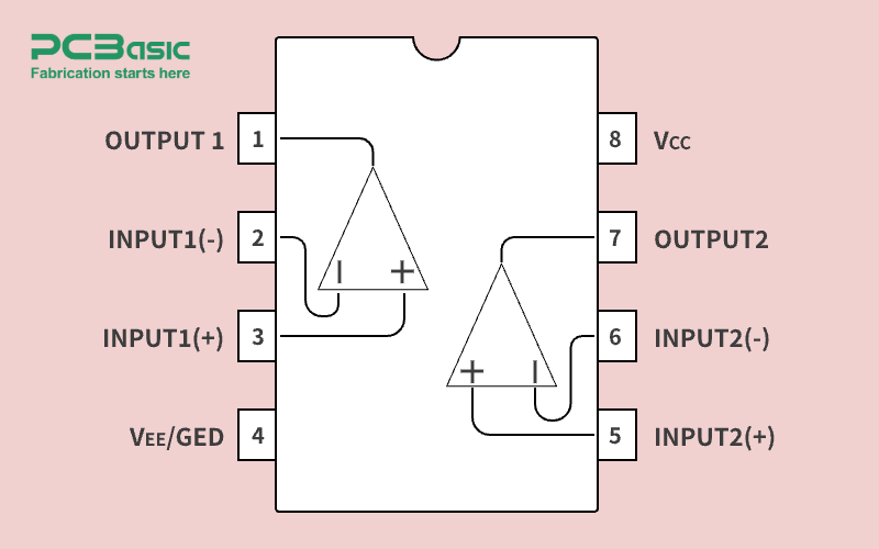
Here is the LM358 pinout for reference:

· Pin 1 (Output - Op-Amp 1): Provides the output from the first operational amplifier.
· Pin 2 (Inverting Input - Op-Amp 1): Receives the inverted input signal for Op-Amp 1.
· Pin 3 (Non-Inverting Input - Op-Amp 1): Receives the non-inverted input signal for Op-Amp 1.
· Pin 4 (Vss - Ground): The ground or negative supply pin, essential for proper operation.
· Pin 5 (Offset Null - Op-Amp 1): Used to adjust any input offset voltage to maintain precision.
· Pin 6 (Output - Op-Amp 2): Provides the output from the second operational amplifier.
· Pin 7 (Inverting Input - Op-Amp 2): Receives the inverted input signal for Op-Amp 2.
· Pin 8 (Non-Inverting Input - Op-Amp 2): Receives the non-inverted input signal for Op-Amp 2.
Pin 1 (Output - Op-Amp 1)
The output pin of Op-Amp 1 delivers the amplified signal. When used in a sensor circuit, such as a circuit with a light-dependent resistor (LDR), this output connects to the next stage, whether it is a voltage comparator or feedback loop, providing feedback from the light sensor.
Pin 2 (Inverting Input - Op-Amp 1)
The inverting input of Op-Amp 1 is where an inverted signal can be fed in. This is particularly useful for processing signals from photo transistors or photo diodes when the phase reversal is needed for correct signal inversion.
Pin 3 (Non-Inverting Input - Op-Amp 1)
The non-inverting input receives the signal in its natural, non-inverted state. When connected to a photo transistor or photo diode, this input ensures the signal remains unchanged and can be amplified directly without inversion, ideal for light-dependent applications.
Pin 4 (Vss - Ground)
This pin provides the ground connection, typically tied to the negative side of the power supply. A stable ground connection is crucial to ensure the proper operation of the op-amp.
Pin 5 (Offset Null - Op-Amp 1)
The offset null pin helps eliminate any small errors or offset voltage present at the input. This is important in sensor circuits where precision is essential, especially in light-dependent applications where small voltage variations can significantly affect performance.
Pin 6 (Output - Op-Amp 2)
This is the output pin for Op-Amp 2. Like Pin 1, it provides an amplified signal, but from the second op-amp. This could be used in applications such as signal conditioning or voltage comparison based on inputs from photo diodes or light-dependent resistors.
Pin 7 (Inverting Input - Op-Amp 2)
This pin receives the inverted input signal for Op-Amp 2. In circuits where signal inversion is required, such as some light sensor circuits, this input pin can be used to condition the signal from photo transistors.
Pin 8 (Non-Inverting Input - Op-Amp 2)
The non-inverting input of Op-Amp 2 works in the same way as Pin 3, receiving the non-inverted input signal and amplifying it. This is particularly useful for sensor circuits designed to detect light levels using light-dependent resistors (LDRs) or photo transistors.
The LM358 is designed to operate with a single power supply, making it ideal for low-power applications.
·Pin 4 (Vss - Ground) is the ground pin, connected to the negative terminal of the power supply.
·Pin 8 (Vdd - Positive Supply) connects to the positive terminal of the power supply. The typical operating voltage ranges from 3V to 32V, depending on the circuit’s needs.
A stable power supply is essential for the LM358 to perform optimally, especially in applications like sensor circuits, where signal stability and amplification precision are crucial.
The LM358 offers several advantages when used in sensor circuits:
· High input impedance ensures it won't load the sensor.
· Low output impedance ensures that the amplified signal can drive the next stage of the circuit effectively.
· Low offset voltage provides accuracy, which is crucial when processing signals from components like photo diodes or light-dependent resistors (LDRs).
In light-sensitive circuits, photo transistors or photo diodes are often used as the primary signal sources. These components change their resistance or voltage based on the light they detect. The LM358 can amplify these weak signals, allowing for more accurate processing and response in light-dependent applications.
Light-Sensitive Sensor Circuits: The LM358 is widely used to amplify signals from photo diodes, photo transistors, and light-dependent resistors (LDRs) in systems such as automatic lighting control or environmental monitoring.
Voltage Comparators: In these configurations, the LM358 can compare input voltages to determine whether certain light thresholds have been reached, triggering actions like turning on lights or adjusting camera settings.
Active Filters: The IC is also used in active filter designs, where it helps filter certain frequencies from an input signal, such as in audio circuits or noise reduction systems.
Signal Amplification: The LM358 amplifies weak signals from photo transistors or photo diodes in various sensing applications, improving their readability and accuracy.
· Signal amplification from sensors such as photo diodes and photo transistors.
· Active filters and voltage comparators for light-dependent circuits.
· Integration into sensor circuits for light or temperature monitoring.
|
Parameter |
LM358 |
LM324 |
TL072 |
LM2904 |
|
Package Type |
DIP-8, SOIC-8 |
DIP-14, SOIC-14 |
DIP-8, SOIC-8 |
DIP-8, SOIC-8 |
|
Operating Voltage Range |
Single supply 3V–32V |
Single supply 3V–32V |
±3V–±18V |
Single supply 3V–32V |
|
Input Bias Current |
Low |
Moderate |
Very Low |
Low |
|
Gain Bandwidth Product |
1 MHz |
1 MHz |
3 MHz |
1 MHz |
|
Features |
Single-supply, low power consumption |
Quad op-amp |
Ultra-low noise |
Automotive-grade version available |
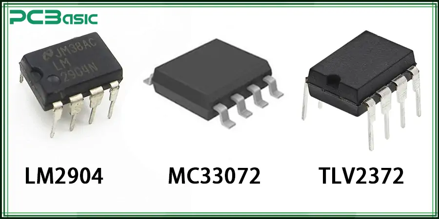
If the LM358 cannot be obtained, you can choose the following chips that are compatible with the functions and pins of the LM358 as alternatives. LM358 equivalent has:

LM2904: Automotive-grade version, suitable for low-voltage applications.
MC33072: An alternative to higher speed and wider bandwidth.
TLV2372: A low-power, rail-to-rail output alternative model.
When replacing the chip, please be sure to reconfirm whether the LM358 SMD pinout or LM358 IC pinout is compatible, especially in high-precision analog signal processing applications.
The LM358 pinout is a simple yet powerful configuration for building a variety of analog systems, especially in sensor circuits where light-dependent signals need amplification. Its ability to operate with a single power supply and its ease of use in low-power applications make it a popular choice for engineers working with photo diodes, photo transistors, and light-dependent resistors (LDRs). By understanding how each pin works and how to integrate it into a circuit, designers can create efficient, reliable, and accurate systems for a wide range of applications, from light-sensitive sensors to voltage comparators.

Assembly Enquiry
Instant Quote
Phone contact

+86-755-27218592
In addition, we've prepared a Help Center. We recommend checking it before reaching out, as your question and its answer may already be clearly explained there.
Wechat Support

In addition, we've prepared a Help Center. We recommend checking it before reaching out, as your question and its answer may already be clearly explained there.
WhatsApp Support

In addition, we've prepared a Help Center. We recommend checking it before reaching out, as your question and its answer may already be clearly explained there.