Global high-mix volume high-speed PCBA manufacturer
9:00 -18:00, Mon. - Fri. (GMT+8)
9:00 -12:00, Sat. (GMT+8)
(Except Chinese public holidays)
Global high-mix volume high-speed PCBA manufacturer
9:00 -18:00, Mon. - Fri. (GMT+8)
9:00 -12:00, Sat. (GMT+8)
(Except Chinese public holidays)
HomePage > Blog > Knowledge Base > How to ensure the quality of BGA welding during PCBA manufacturing by using X-RAY inspection equipment.
inseparable from the PCBA fabrication process.
manufacturing.
of BGA.
requirements. In other words, with the continuous upgrading of PCB chip, the production capacity of PCB assemblers should also increase.
partner.
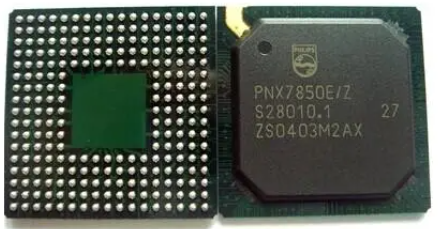
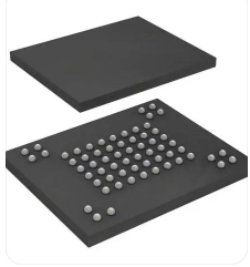
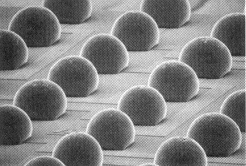
The full name of BGA is Ball Grid Array, which is a packaging method of chips. BGA has
many advantages, such as:
1. Small size, thickness and weight of BGA package.
2. The contact surface between the array solder balls of the BGA and the substrate is
3. large and short, which is conducive to heat dissipation.
4. The pins of the BGA array solder balls are very short, which shortens the signal
transmission path.
More stable than other packages, no risk of bending and breaking pins.
Better thermal conductivity and less power consumption.
Because of these characteristics of BGA, it is widely used in notebook CPU,
smartphone CPU, smart watch applications, medical equipment, solar control systems,
robots, car and industrial control applications and other consumer goods such as
canner, projector, image processor, temperature sensor , graphics card, etc.
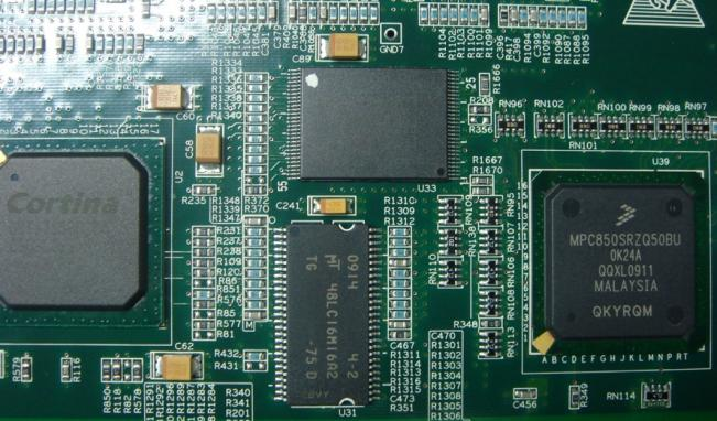
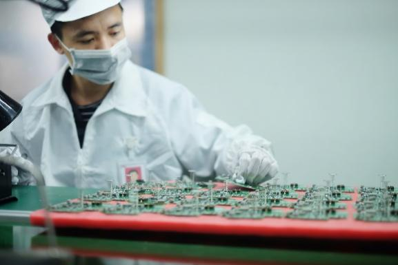
The many advantages of BGA directly promote companies to adapt the innovative
package design to their products, the application of BGA components become more
widely used over time. Many new products will use multiple BGA integrated circuits and
components in a single design, but nothing is perfect and BGA has a disadvantages
that cannot be ignored. The first and foremost disadvantage is the quality and reliability
of solder joints after soldering, Once the BGA successfully welded to the PCB board, it’s
difficult to guarantee the quality of welding due to the BGA package design. The
inspection difficulty increases for PCBA manufacturers thus there is a need in innovative
solutions and approach to ensure quality and consistency over time.
BGA solder joints at the bottom of the component cannot be inspected and judged by
ordinary equipment such as AOI and microscopes, which are often used in SMD PCBA
fabrication. For that reason, it is necessary to verify the quality of every stage in the
BGA production process to ensure consistency and quality of the finished product.
The BGA quality assurance can be done in multiple stages:
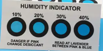
Every BGA package comes with “humidity card” a small card that changes colors based
on chemical reaction if the humidity raise above a certain level. When the original
packaged chip is unpacked from it’s original vacuum sealing, the humidity card will show
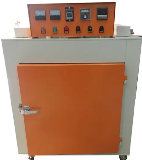
that the chip must be baked if the humidity exceeds 30%. According to the standard
operation specification of oven baking, the temperature is generally set at 100-120 ℃,
and the baking time is 8-12 hours. The function of baking is to dry the moisture absorbed by the chip in the open air. Otherwise, the bubbles that caused by humidity
and air may damage the chip when the SMT patch passes through the reflow soldering
process at a temperature of 240 °C.
In the SMT PCBA process, there will be multiple BGA products in every production line.
For that reason, multiple equipments such as automatic printing machine and SPI
solder paste inspection machine are necessary in order to facilitate the production and
SMT of BGA components.
Since the solder joints of BGA are at the bottom, BGA solder joints cannot be visually
inspected, and AOI machinery also can’t be used once the placement has finished. it is
necessary to ensure the quality of the SMT placement before the placement to avoid
unnecessary complications. Every quality PCBA manufacturer knows that it is
prerequisite to take good care and do a good job during the BGA SMT process which
ensures the integrity and the accuracy of solder paste printing.
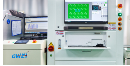
Another necessary machine is the SPI machine that checks and ensure the printing
quality. Once the SPI machine has successfully accomplished the test, a green “OK” will
show up on the placement machine. If the PCBA manufacturer doesn’t use SPI
inspection during the BGA pad printing and solder pasting process, there will be tin-placement issues such as not enough tin, or too much tin pasted during the SMT
process.
SPI machinery is necessary when it comes to BGA SMT fabrication, without SPI test,
short circuit and other malfunctions might occur, which will eventually affect the function
and the quality of the assembled product.
Due to the special spherical contact arrangement of the BGA, its solder joints are
invisible, and the process specification is difficult. For such reasons, It is impossible to
perform manual or visual inspection by using an equipment such as optical microscope
and even the AOI machine.
All those machineries and techniques cannot detect the solder joints at the bottom. How
do we perform BGA testing then? The answer is detection with the help of X-Ray
equipment.
After welding the BGA on top of the PCBA, engineers need to use X-RAY equipment to
check and verify the welding quality. IPQC (process quality control) standard is to
conduct random inspections every hour or 10% of the time in normal production
environments.
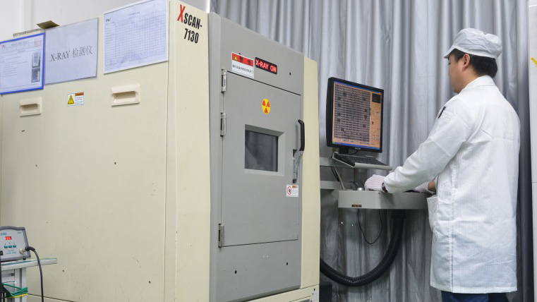
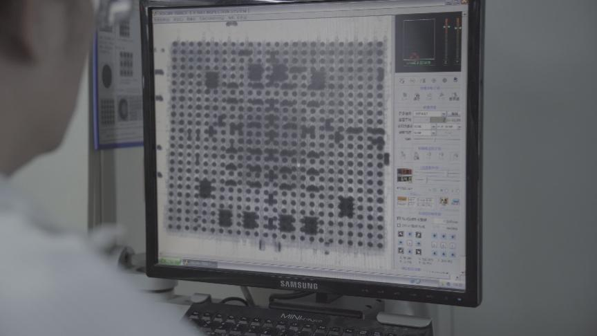
The biggest advantage of X-Ray inspection equipment is that it can monitor all solder
joints on the circuit board, including solder joints that are invisible to the human eye. XRay can detect solder joint defects in BGA, such as voids, desoldering ( Open circuit),
bridging (short circuit), cold soldering, incomplete melting of solder balls, displacement,
solder beads; and whether there are air bubbles. insufficient solder volume and other
defects, cannot be detected by AOI, therefore, We use X-Ray for BGA once it’s already
mounted and welded on top of the circuit board. the advantages of X-Ray inspection
equipment are shown below:
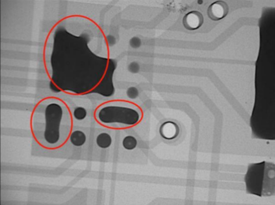
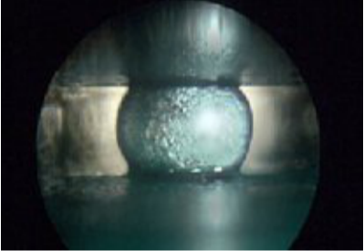
short circuit due to too much tin placement Tin point does not melt
PCBA products with BGA mounting need to have a complex management process
systems and sophisticated hardware equipment for verification and integrity insurance
purposes.
Only with SPI and X-RAY testing equipment can the mounting quality of BGA be
guaranteed.
SPI and X-ray testing equipment is of practical significant technique to ensure the
quality fault prevention during the BGA component assembly process. Some small
factories are reluctant to invest in these testing equipment, but at PCBasic quality is
above everything.
If you want to know more about PCBA manufacturing and BGA welding, feel free to
follow us and learn more.
PCBasic constantly post and share information related to PCB proofing, SMT patch and
PCBA processing related needs. If you have any request, question or a story to share -
you can always contact us through the message box on the right side of the site.

Assembly Enquiry
Instant Quote
Phone contact

+86-755-27218592
In addition, we've prepared a Help Center. We recommend checking it before reaching out, as your question and its answer may already be clearly explained there.
Wechat Support

In addition, we've prepared a Help Center. We recommend checking it before reaching out, as your question and its answer may already be clearly explained there.
WhatsApp Support

In addition, we've prepared a Help Center. We recommend checking it before reaching out, as your question and its answer may already be clearly explained there.