Global high-mix volume high-speed PCBA manufacturer
9:00 -18:00, Mon. - Fri. (GMT+8)
9:00 -12:00, Sat. (GMT+8)
(Except Chinese public holidays)
Global high-mix volume high-speed PCBA manufacturer
9:00 -18:00, Mon. - Fri. (GMT+8)
9:00 -12:00, Sat. (GMT+8)
(Except Chinese public holidays)
HomePage > Blog > Knowledge Base > Common PCB problems
PCB and PCBA are ubiquitous these days, and PCB problems are unavoidable. Printing pcb and PCBA production can be very tedious. In this article, we will cover the most common PCB problems. We will cover the cause of the PCB problems, how to avoid them and how to solve issues as they occur. By following our guide, you'll be able to recognize these PCB problems early and solve them promptly.
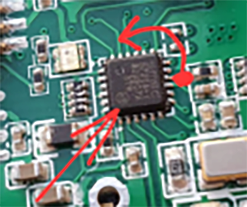
One of the most common PCB problems is a burned circuit board. This problem occurs when one or more components fail due to a short circuit, faulty component, or bad soldering. Once such a problem occurs. Sometimes, it might require a replacement of the entire PCB circuit board. You might be wondering: how to tell if a circuit board is bad? here are a few tips on how to find a short on a circuit board:
In normal circumstances and procedures, each circuit is carefully checked before being plugged into the power. Not only it's dangerous not to limit the components carefully, but it could damage the entire circuit board and require a new PCBA.
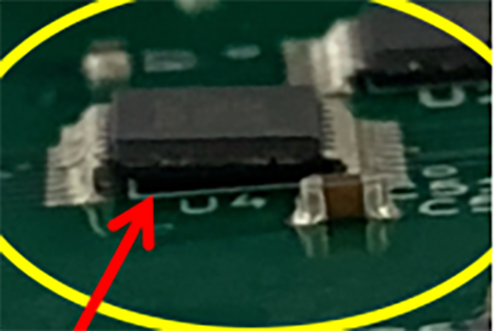
One of the most common PCB problems comes from the components themselves. During the PCBA process, there are a lot of uncertainties. We can eliminate those uncertainties by following the best procedures and sourcing the ingredients from a trusted supplier/distributor. A poorly manufactured component is a crucial reason the PCBA might fail during tests. There are certain things we can do to ensure the common PCB problems related to details won't occur:
By following those steps, we can detect poorly manufactured components early and prevent them from reaching the mass production process.
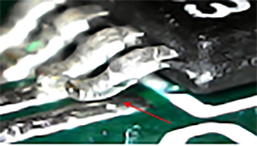
It might sound like an easy problem to fix, but it might be quite a journey to find. Bad soldering is a significant cause of specific PCB issues, especially during an early prototype stage.
During the prototyping stage, the sample board is soldered by hand, which will inevitably cause-specific soldering issues. Those issues sometimes come in the form of unsafe operation of components or even complete inability to use specific circuits. In some extreme cases, lousy soldering can cause foul heat dispense, resulting in a burned circuit board.
Things you could do to prevent lousy soldering of components include:
The most common way to test whenever your circuit has harmful soldered components is by using a multimeter. Using the multimeter, navigate the settings to check short courses. By using this feature, you will detect whenever a circuit is open or closed. If the circuit is left empty, it could indicate a bad solder joint is involved. Although, a possibility of PCB layout-related issues could persist, which will require a further check by the PCB engineer.
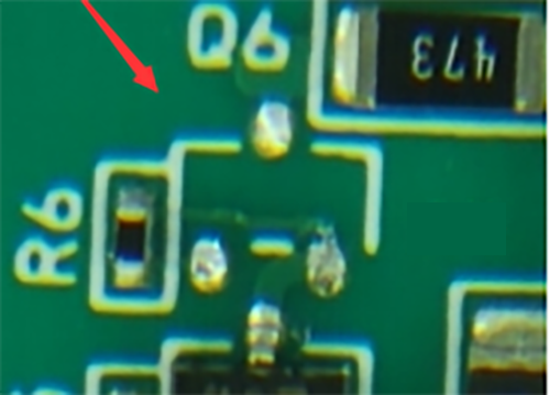
Another common PCB problem might not be related to the PCB circuit itself but the environmental factors surrounding it. PCB and components, in particular, have specific storage and operation environment. Each component manufacturer states the ecological factors that could impact the members in the component's datasheet. such factors could be:
Certain factors don't necessarily result in damaged components or the inability of a circuit to operate. But, sometimes, those environmental factors and conditions could impact the product's lifespan and quality.
It's essential to follow the component's datasheet and choose appropriate details for the product use case. For example, if the product is designed for industrial applications, certain conditions such as high temperature and humidity should be met.
A common PCB issue might arise by not checking the component or the PCB production date. Similar to other products in life, PCB and components have shelf-life too.
The shelf life of components and printed circuit boards can vary from a few months to a few years. Shelf life usually depends on the storage conditions assigned by the component manufacturer; those could vary based on environmental impacts and storage conditions.
The components are usually purchased and delivered in a vacuum-sealed package. Once unpacked, the details need to be placed and assembled as soon as possible. In an unsealed vacuum package, the components will be exposed to oxygen, which reduces the components' shelf life and quality over time.
Another factor the age refers to is the operational age of the components. Depending on the application, members have a certain lifespan that could start from a few months up to 10 years or more. This age is reduced under different environmental factors. As long as the board operates under normal conditions, the datasheet lifespan information is usually very accurate.
Plating voids usually refer to a group of PCB issues that occur on the PCB plates (layers) through the manufacturing process or after the PCBA fabrication process. There are many issues and causes for plating voids, and most of them will lead to the same result: PCB board which is vulnerable to cracks and damage once exposed to different stressful environments such as pressure, vibration, heat, and so on…
Although no direct solution exists for plating voids, many things can be done to detect PCB boards with holes early. The most efficient solution is to discard the board and prevent them from getting into the PCBA assembly line.
Although not a common PCB issue, PCB designers and engineers often make this mistake. An insufficient copper-to-edge clearance occurs when the PCB layout routing is too close to the edges of the PCB. This could cause signal and power-related issues that sometimes are difficult to detect and resolve.
"trimming" refers to cutting the PCB edges in a particular shape according to the PCB design. If the layout routing is too close to the edge, it might also be trimmed. The best practice will be to avoid getting too close to the border during the PCB layout and design process and avoid unnecessary PCB issues.
Not a PCB issue directly but a method that could prevent possible PCB issues. Immersion of silver is the process of submerging the PCB in silver liquid to protect it from oxidation and other environmental-related damages. Those environmental effects usually occur once the PCB is unsealed and used for quite some time.
The immersion silver is offered free of charge during the PCB fabrication process. The process is RoHS certified and environmentally friendly. It's preferable to the traditional lead finish, which badly impacts the environment.
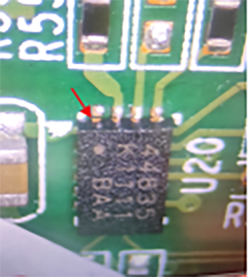
Many common PCB issues are related to the PCB design. A missing solder mask between the pads is just another one of them. Luckily, missing solder masks are very easy to identify either through simulation software or visual inspection. Once identified, The engineer will correct it reasonably quickly, but that mistake might require producing a new PCB board. It's essential to pay attention to the possibility of such common PCB issues to save time and cost in the PCBA fabrication process.
Although it might not sound like a common PCB issue, it is more common than most people think. Acid trap refers to a situation where the PCB layout includes sharp edges, which might result in trapped chemicals in the cooper layers of the printed circuit board. Sharp layout edges can cause acid traps, bad quality signal transfer, and insufficient power issues. This issue is easily avoidable by ensuring the layout is done right and discarding any sharp edges during the design process. It's crucial to ensure the layout is correct and wired adequately before sending the PCB files to fabrication.
In the article, we covered most of the common PCB mistakes and PCB issues that could arise by either designing the PCB or delivering it to fabrication in a PCBA factory. Most if not all the problems are preventable. All we need is to pay attention to them.
PCBasic offers one-stop services from design services to PCB fabrication, components purchasing, and PCB assembly. Using a one stop pcba service can avoid most, if not all, the mistakes above. Whenever your project is in the prototype or mass production stage, we would love to hear from you and offer you the best service possible for the best market price. Ask for a quotation now and get your PCB and PCBA fabricated today!

Assembly Enquiry
Instant Quote
Phone contact

+86-755-27218592
In addition, we've prepared a Help Center. We recommend checking it before reaching out, as your question and its answer may already be clearly explained there.
Wechat Support

In addition, we've prepared a Help Center. We recommend checking it before reaching out, as your question and its answer may already be clearly explained there.
WhatsApp Support

In addition, we've prepared a Help Center. We recommend checking it before reaching out, as your question and its answer may already be clearly explained there.