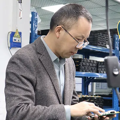
In modern electronic manufacturing, precision and efficiency are the core elements that drive the successful mass production of high-performance products. With the continuous development of electronic products towards miniaturization, high density and high speed, the requirements for soldering quality are also getting higher and higher. In SMT, the circuit board stencil is one of the key tools for achieving high-quality soldering.
A circuit board stencil—also referred to as a solder paste stencil or PCB stencil—is used to coat solder paste before surface mounting. Its thickness, material, opening design, etc., will affect both the amount and accuracy of solder paste deposition. It is not merely a tool, but also one of the key factors determining success or failure in the electronic manufacturing process.
In this article, we will provide you with a comprehensive analysis:
What is a PCB Stencil?
Common types of stencils and their application scenarios
Mainstream stencil manufacturing methods such as laser cutting, chemical etching and electroforming
Comparison of the use of different materials (such as stainless steel and nickel) in PCB stencils
How to choose the appropriate thickness of stencil and opening structure according to product design
Common high-quality PCB stencil manufacturers in the industry and selection suggestions

What is a Circuit Board Stencil
A circuit board stencil is a kind of thin metal sheet used for precisely printing solder paste onto the solder pads on the surface of the printed circuit board. It is usually made of stainless steel and has openings precisely cut by laser to correspond to the PCB pads. There are several types of PCB stencils available. Among various types of PCB stencils, laser-cut stencils are widely adopted due to their high precision and consistency.
The main function of the circuit board stencil is to precisely control the deposition position and volume of the solder paste to ensure that each pad receives the correct amount of solder paste. During use, engineers will align the stencil with the PCB through fiducials. Then the metal squeegee of the solder paste printer will evenly scrape the solder paste over the surface of the stencil. The solder paste will then deposit onto the PCB pads through the openings. After removing the stencil, the PCB can proceed to the surface mount and reflow soldering processes. Among them, solder stencil thickness is the key parameter that determines the volume of solder paste. Excessive thickness may cause problems such as excessive solder paste and bridging. If it is too thin, it may lead to false soldering at the solder joints and the soldering will not be firm.
The advantages of using PCB stencils in SMT production lines are:
Apply the solder paste precisely onto the SMT pads
The formed solder joints are more consistent and reliable
Soldering defects, such as solder bridges, tombstones, and voids, can be reduced
The efficiency and yield of the automated production line can be improved
High-performance circuit board stencil is an indispensable part of modern SMT production lines. Selecting the appropriate stencil based on parameters such as circuit board layout, opening design, material selection and stencil thickness is crucial for ensuring assembly quality. Next, let's take a look at the manufacturing process of the circuit board stencil.

How PCB Stencils Are Made
High-quality circuit board stencil needs to be manufactured through precise engineering processes, including digital design, precise cutting and surface treatment. The following is the typical manufacturing process of PCB stencils:
1. CAD file preparation

The first step in stencil manufacturing is to prepare the CAD design documents. The format of the file is usually Gerber format. These documents define the position, size and shape of each opening on the stencil. During the PCB design stage, a dedicated stencil layer is generated to ensure that the final fabricated soldering stencil is precisely aligned to the SMT pads of the printed circuit board.
In the design process of PCB stencil, key parameters such as the thickness of the solder stencil, pad area and component spacing need to be comprehensively considered. And it is necessary to closely cooperate with the PCB designer so that the holes opened out will be moderate, avoiding excessive or insufficient solder paste during the printing process.
2. Manufacturing process
After the design is completed, the stencil will be officially fabricated according to the process method. At present, the mainstream manufacturing methods for circuit board stencils include:

Laser-cut stencil
Laser cutting stencil is currently the most commonly used manufacturing process for stencils. It precisely cuts each opening through a high-speed laser. The holes opened can achieve micron-level precision and have smooth hole walls, making them highly suitable for high-density SMT packaging. Almost all professional PCB stencil manufacturers adopt this process to manufacture stencils.
Electroforming
Electroforming is a process in which nickel is deposited on a substrate through an electrochemical deposition technique to form open areas. This type of electroformed solder stencil has extremely smooth hole walls. The solder paste has excellent release performance and is suitable for electronic products with micro-pitch and high reliability requirements (such as medical equipment, avionics, etc.).
Chemical Etching
Chemical etching is a traditional process that uses chemical solutions to etch steel sheets to form holes. This process has a low cost but poor precision and is not suitable for precision surface mount components.
3. Surface treatment

To enhance the performance and lifespan of SMT stencils, PCB stencil manufacturers often carry out surface treatment on them. It mainly includes:
Hole wall polishing: Further smooth the interior of the open hole, improve the release of solder paste, and reduce the phenomenon of hole blockage.
Nano-Coating: It forms a hydrophobic layer on the stencil, which can significantly improve the demolding effect of solder paste and reduce the cleaning frequency.
These treatment measures can significantly improve the printing consistency and service life of solder paste stencils.
Materials Used in PCB Stencils
After understanding the stencil manufacturing process, we need to have an in-depth understanding of the materials used to manufacture this type of circuit board stencil. The material selection of the stencil will directly affect the performance, durability of the stencil and the quality of the solder paste stencil. Commonly used stencil materials include:
Stainless steel

Stainless steel is the most commonly used material in the manufacturing of PCB stencils. It is renowned for its high strength, fine grain structure and excellent corrosion resistance. This material ensures that the opening size of each solder paste stencil is consistent and the printing effect is stable, which is very suitable for high-density SMT stencils.
Nickel-plated stainless steel
To further enhance wear resistance and solder paste release effect, some PCB stencil manufacturers will use nickel-plated stainless steel materials. The inner wall of the stencil of this material is smoother, which is more conducive to the release of solder paste.

Polyimide or Mylar
In the low-cost or prototype making stage, flexible materials such as Polyimide or Mylar are also used to make prototype stencils. Although these materials are not as durable as metals, they are suitable for small-batch printing or calibration use. This type of stencil is usually cut by die-cutting rather than laser cutting and is widely used in DIY enthusiasts or teaching and experimental scenarios.
The thickness of the solder stencil plays a crucial role in solder paste release. The common thickness range is between 0.1mm and 0.2mm, depending on the size of the pads, the spacing and the type of components. Fine-pitch components use a thinner stencil, while larger pads or through-hole printing are suitable for a thicker stencil.
Types of PCB Stencils
The several common types of PCB stencils in electronic manufacturing mainly include:
1. Framed Stencils

A framed stencil is also known as a fixed stencil. This stencil is permanently installed on the metal frame and is widely used in the automatic stencil printing machines of large-scale SMT production lines. The main features of this type of stencil are stable tension, strong durability and high alignment accuracy. As shown in the picture:
2. Frameless Stencils

This type of stencil is a frameless loose sheet material, featuring high flexibility and lower cost. It is particularly suitable for medium and small batch production or product sampling. This type of stencil is suitable for manual or semi-automatic printing. As shown in the picture:
3. Prototype Stencils

The prototype stencil is a type of stencil designed for engineering development and initial testing. It is usually frameless in structure and economical and practical. This type of stencil is suitable for short-batch, small-scale sampling, functional verification, etc. As shown in the picture:
4. Electroformed Stencils

Electroplated stencil is a high-end stencil manufactured by the electroforming process. It has excellent solder paste release performance and is suitable for high-density fine-pitch packaging. As shown in the picture:
Stencil Design Considerations
When designing a stencil, there are many aspects that need to be taken into consideration. Here are some aspects we have summarized that need to be considered during design:
|
Design Factor
|
Description
|
Purpose & Impact
|
Recommended Practice
|
|
Aperture Size and Shape
|
Refers to the size and shape of each stencil opening, which determines the amount of solder paste applied during printing.
|
Openings that are too small may lead to insufficient solder and weak joints; too large may cause bridging or shorts.
|
Adjust aperture dimensions according to the pad size and component pitch. Use CAD tools with Gerber files for optimization.
|
|
Wall Smoothness and Taper
|
Indicates whether the aperture walls are smooth and slightly tapered, which affects solder paste release.
|
Rough or vertical walls can lead to solder paste residue or incomplete printing.
|
Use laser-cut stencils or electroformed stencils to ensure smooth aperture walls and consistent solder paste release.
|
|
Pad-to-Aperture Alignment
|
The stencil aperture must be precisely aligned with the PCB pads to avoid solder paste misalignment.
|
Misalignment can cause component shifting or weak solder joints, affecting overall PCBA quality.
|
Use professional PCB design software to align Gerber files accurately and select high-precision stencil fabrication.
|
|
Fiducials for Alignment
|
Visual alignment marks are placed on the stencil for recognition by pick-and-place machines.
|
Helps improve machine vision accuracy and ensures precise component placement during SMT assembly.
|
Include at least three fiducial marks on the stencil that correspond with fiducials on the PCB for optimal alignment.
|
|
Stencil Thickness Selection
|
A key parameter that determines the thickness of the solder paste applied—typically ranges from 0.1mm to 0.2mm.
|
Too thick → bridging; too thin → insufficient solder. Must be adjusted based on component type and pad size.
|
Common guidelines:- 0.12mm: for 0402/0603/0805 standard components- ≤0.1mm: for 01005, BGA, fine-pitch parts- ≥0.15mm: for power components and large pads
|
How to Use Circuit Board Stencil
Using a PCB stencil is a key step in SMT, ensuring accurate solder paste printing before component placement and reflow soldering. The following are the usage steps for manual solder paste printing:
1. Preparatory Work
Ensure that the working environment is clean and dust-free, and take good anti-static measures.
Prepare tools such as stencil, solder paste, scrapers and positioning fixtures.
Place the PCB circuit board steadily on the platform or special fixture to ensure it is firmly fixed and not easy to move.
2. Align the PCB with the PCB stencil
Carefully cover the stencil of the circuit board above the PCB.
Carefully adjust the stencil to ensure that the openings are accurately aligned with the pads on the PCB.
If a framed stencil is used, alignment accuracy can be improved by means of positioning holes or fiducials.

3. Apply solder paste by scraping
Use a stainless steel or plastic scraper to evenly apply solder paste on the surface of the stencil.
Maintain an angle of about 45 degrees and apply appropriate pressure to smoothly push the solder paste through all the openings.
Ensure that the solder paste is evenly filled in each hole without any voids or accumulation.
4. Remove the stencil
After the solder paste printing is completed, lift the PCB stencil slowly and vertically to avoid lateral movement.
Check whether the solder paste is evenly covered on the pads, without any stringing, offset or bridging phenomena.
5. Check the printing effect of solder paste
Use a magnifying glass or AOI to check the paste condition of each solder joint.
Ensure that the solder paste pattern on each pad is complete, clear, and free of residue or overflow.
Following the reflow temperature profile, the solder paste melts and forms a strong solder point, completing the soldering process.
At this point, the solder paste is printed. If an automatic solder paste printer is used for printing, the operation process is almost the same. Machine printing will be simpler. Whether it is prototype prototyping or mass production, using high-quality PCB stencils can achieve precise solder paste printing, reduce rework rates, and improve SMT assembly efficiency and yield. So, how can we know if the stencil is of high quality?
A Reliable PCB Stencil Manufacturer - PCBasic

To ensure that the stencil used is of high quality, one can choose a reliable PCB stencil manufacturer. PCBasic is one of the reliable circuit board stencil manufacturers in the industry. It can provide high-quality and customized circuit board stencils, meeting various needs of customers from sample making to mass production.
PCBasic can provide a complete series of PCB stencil products, including framed stencil, frameless stencil, laser cut stencil, electroformed stencil, etc. As an experienced PCB stencil maker, each of its solder paste stencils undergoes strict tolerance control and open polishing treatment. Each stencil has excellent durability.
PCBasic can also precisely optimize the opening design of each soldering stencil, pad alignment and solder stencil thickness (typically 0.1mm to 0.2mm) based on the Gerber file provided by the customer. PCBasic is equipped with advanced devices and has a strict quality inspection process. Whether it is BGA, QFN, 01005 micro-components or conventional surface mount devices, the solder paste printing effect it brings is precise and repeatable.
Conclusion
Circuit board stencil plays a crucial role in the SMT assembly process. It directly affects the soldering quality, assembly efficiency and the reliability of the final product. The correct selection of solder paste stencil (including its thickness, opening design, and material type) can significantly reduce soldering defects such as solder bridging, tombstoning, and cold joints. To ensure the stability and consistency of solder paste printing, it is crucial to cooperate with a professional PCB stencil manufacturer. As an experienced manufacturer, PCBasic possesses advanced stencil manufacturing technology and can provide a complete set of stencil solutions for circuit boards suitable for prototyping and mass production.
A high-quality PCB stencil is not only a tool but also a key guarantee for the success of modern electronic manufacturing.
 About PCBasic
Time is money in your projects – and PCBasic gets it. PCBasic is a PCB assembly company that delivers fast, flawless results every time. Our comprehensive PCB assembly services include expert engineering support at every step, ensuring top quality in every board. As a leading PCB assembly manufacturer, we provide a one-stop solution that streamlines your supply chain. Partner with our advanced PCB prototype factory for quick turnarounds and superior results you can trust.