Global high-mix volume high-speed PCBA manufacturer
9:00 -18:00, Mon. - Fri. (GMT+8)
9:00 -12:00, Sat. (GMT+8)
(Except Chinese public holidays)
Global high-mix volume high-speed PCBA manufacturer
9:00 -18:00, Mon. - Fri. (GMT+8)
9:00 -12:00, Sat. (GMT+8)
(Except Chinese public holidays)
HomePage > Blog > Knowledge Base > Understanding Blind Vias in PCBs: A Complete Guide
Printed circuit boards, or PCBs, are everywhere. They power your phone, laptop, smartwatch—almost every piece of modern technology. But inside these tiny boards is a complex network of connections. One of the key players in this network is PCB via.
Vias are tiny holes that let electrical signals travel between layers of a PCB. Some go all the way through the board. Others stop halfway. The ones that stop halfway are what we call blind vias.
They’re small, but they do a big job. And if you’re designing high-density electronics, you need to understand them. This guide will break down what they are, how they’re made, and when to use them.
Read on!
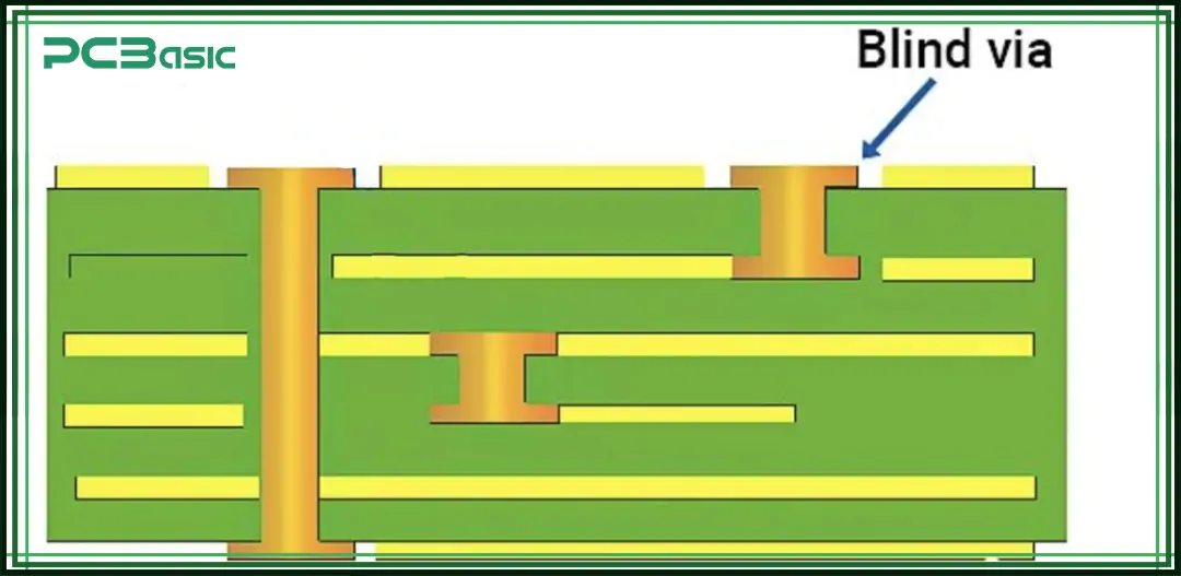
Let’s start with the basics. A via connects one layer of a PCB to another. Think of it as a vertical wire inside the board. It’s how different layers connect to each other.
Now, there are three main types of PCB vias:
• Through-hole vias: go from top to bottom through the entire PCB.
• Blind vias: connect an outer layer to an inner layer, but not all the way through.
• Buried vias: connect two or more inner layers. They never reach outside.
Blind vias are called "blind" because they don’t go all the way. You can’t see the other end from the outside.
They are drilled partway into the board, either from the top or the bottom. They save space and let designers pack more into less. That’s why they’re common in HDI (high-density interconnect) boards.
If you're working with blind via PCBs, you’ll see a big difference in routing flexibility. You can squeeze in more components. More signals and less space.
Blind vias aren’t as simple as drilling a hole. Making them takes more time. Plus, more precision and cost.
There are two common methods to create them:
1. Laser drilling
2. Mechanical drilling with controlled depth
Laser drilling is more common in HDI PCBs. It’s fast, clean, and great for tiny holes. However, it’s also expensive.
Mechanical drilling works for larger holes. It uses depth control to stop at the right layer. But it’s slower, and it wears out the tools.
After drilling, the via is plated with copper. This allows electricity to pass through. If this plating fails, the circuit breaks.
That’s why manufacturing blind vias requires tight control. You need skilled engineers and precise machines.
Also, remember this: the more layers you have, the harder it gets. Blind vias in 8-layer or 10-layer boards are advanced work.
The process may involve sequential lamination. That means building the board in steps and adding layers one by one. Each lamination step adds time and cost.
So, if your project doesn’t need blind vias, don’t use them. However, if space and performance matter, they might be worth it.
 About PCBasic
Time is money in your projects – and PCBasic gets it. PCBasic is a PCB assembly company that delivers fast, flawless results every time. Our comprehensive PCB assembly services include expert engineering support at every step, ensuring top quality in every board. As a leading PCB assembly manufacturer, we provide a one-stop solution that streamlines your supply chain. Partner with our advanced PCB prototype factory for quick turnarounds and superior results you can trust.
Here’s where things get technical. Every via has a depth and a diameter. The aspect ratio is the ratio of depth to diameter.
Let’s say your via is 0.2 mm wide and 0.6 mm deep. That’s a 3:1 aspect ratio.
For a blind via, a lower aspect ratio is better. Because plating copper inside a deep, narrow hole is hard. The deeper the hole, the harder it is to coat it evenly.
Most manufacturers prefer a ratio of 0.75:1 to 1:1 for blind vias. Some go up to 1.5:1, but that's pushing it.
A high aspect ratio increases the chance of:
• Voids (air gaps)
• Poor plating
• Cracks under thermal stress
These failures can ruin the whole board.
So, when you design a PCB blind via, always consider the aspect ratio. Choose dimensions your fabricator can handle and talk to them early.
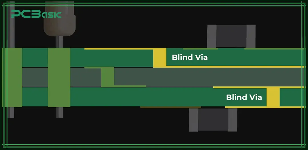
Why do engineers use blind vias? The answer is simple—they save space. In modern electronics, space is gold.
Here are some common use cases:
• Smartphones: Thin boards, complex circuits
• Wearables: Tight packaging, flexible layouts
• Medical devices: Small, precise, reliable
• Military and aerospace: High performance, limited space
• HDI PCBs: More signals per square inch
By connecting only the layers you need, blind vias free up real estate. This reduces the need for long traces, minimizes signal interference, and enhances overall performance.
They also allow for better signal integrity. Shorter paths mean faster signals and fewer problems.
If you're designing a blind via PCB, these vias become a powerful tool to simplify routing and improve performance.
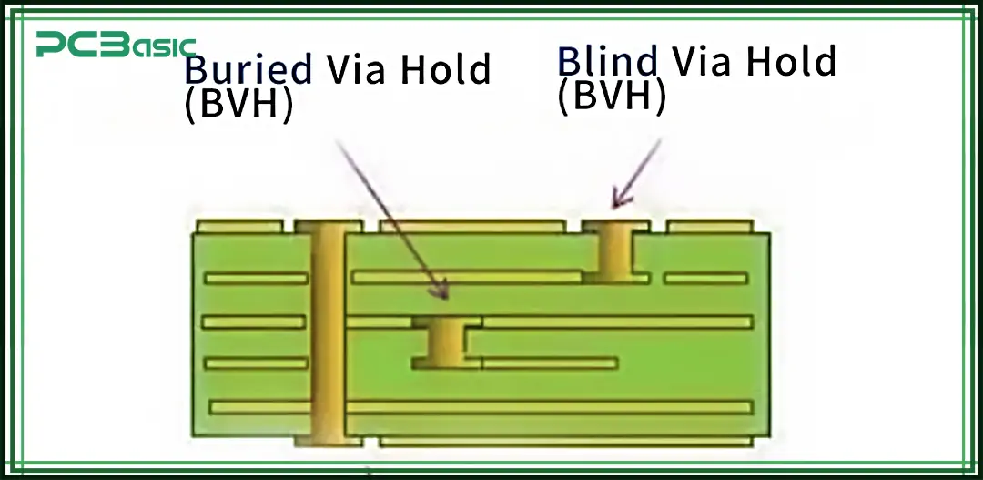
Let’s compare them side by side.
|
Feature |
Blind Vias |
Buried Vias |
|
Visibility |
Visible from one surface |
Not visible externally |
|
Connection |
Outer layer to inner layer |
Inner layer to inner layer |
|
Manufacturing Complexity |
High |
Very high |
|
Used in |
HDI boards, mobile devices |
Complex multilayer PCBs |
|
Cost |
Expensive |
More expensive |
|
Fabrication Process |
Laser/mechanical drilling |
Sequential lamination |
Many advanced boards use a combination of blind vias and buried vias to achieve higher density and better signal management.
Blind vias are simpler than buried vias—but still advanced. You’ll often see both in the same design, especially in high-end products.
They are sometimes grouped as blind and buried vias, especially in fabrication quotes.
Use them together for the best routing options. But keep your budget in mind.
Blind vias are a small part of PCB design—but a critical one. They connect layers without going through the entire board. That makes them perfect for high-density layouts.
However, they come with challenges, such as complex manufacturing, high costs, and strict aspect ratio limits. If you're working on smartphones, medical gear, or aerospace systems, blind vias might be your best friend. They let you do more with less. But if your design is simple, skip them. Regular through-hole vias are easier and cheaper.
In short, it is important to know when to use blind vias and when not to. Always talk to your PCB manufacturer. Share your layer stack-up, your via sizes, and your goals. They’ll help you find the best path forward.
And never forget the basics. Keep your via aspect ratio in check. Choose the right via for the job. Lastly, test your boards since reliability matters.

Assembly Enquiry
Instant Quote
Phone contact

+86-755-27218592
In addition, we've prepared a Help Center. We recommend checking it before reaching out, as your question and its answer may already be clearly explained there.
Wechat Support

In addition, we've prepared a Help Center. We recommend checking it before reaching out, as your question and its answer may already be clearly explained there.
WhatsApp Support

In addition, we've prepared a Help Center. We recommend checking it before reaching out, as your question and its answer may already be clearly explained there.