Global high-mix volume high-speed PCBA manufacturer
9:00 -18:00, Mon. - Fri. (GMT+8)
9:00 -12:00, Sat. (GMT+8)
(Except Chinese public holidays)
Global high-mix volume high-speed PCBA manufacturer
9:00 -18:00, Mon. - Fri. (GMT+8)
9:00 -12:00, Sat. (GMT+8)
(Except Chinese public holidays)
HomePage > Blog > Knowledge Base > Mastering FPGA Design: The Ultimate Guide
In the field of electronics and digital systems, FPGA design has become an extremely important and dynamic technical direction. With the continuous development of technology, field programmable gate array (FPGA) demonstrates extremely high flexibility, fast processing capabilities and powerful customization functions. FPGA chips can flexibly change the hardware structure according to different demands, which is incomparable to traditional chips. Whether you are an aspiring FPGA engineer, a student, or an FPGA engineer with many years of development experience, learning and mastering FPGA design can lay a solid foundation for you to enter popular fields such as embedded systems, artificial intelligence, and telecommunications.
This blog aims to provide you with a complete beginner's and advanced guide to FPGA design. We will introduce in detail the basic principles, core components, main advantages and disadvantages of FPGA, and also explain common FPGA applications in combination with practical cases. Meanwhile, this article will also systematically sort out the essential tools required for FPGA design and each step, helping you quickly get started with FPGA programming. After reading this blog, you will understand why FPGA design and FPGA programming have become one of the most worthy core skills to learn in the current electronics industry.
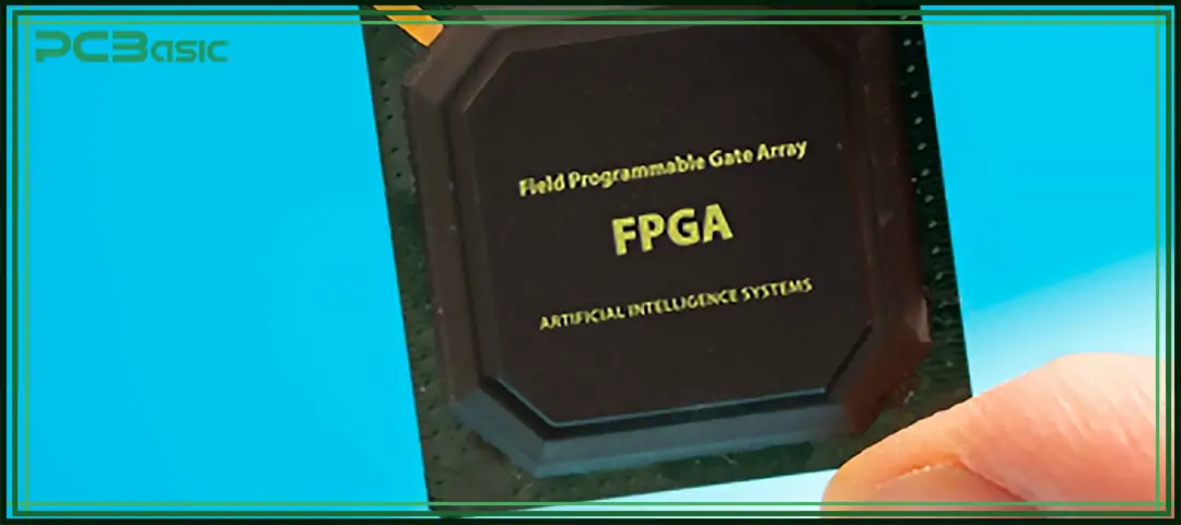
The full name of FPGA is Field Programmable Gate Array. It is an integrated circuit that users can configure and reprogram according to their actual needs after manufacturing. Unlike the fixed-function ASICs (Application-Specific Integrated Circuits), the FPGA chip can be programmed through FPGA programming, performing a variety of different tasks.
"Field programmable" means that users can modify the logic functions of the FPGA at any time after the product is put into actual application. This makes FPGAs very useful in rapid prototyping, repeated testing, and projects that require flexible upgrades.
In simple terms, an FPGA is like a digital canvas. Developers can use dedicated FPGA software to customize hardware functions, run complex algorithms, and adjust the hardware structure as needed. Because of this high degree of programmability, FPGA design has become very important in the field of technological innovation.
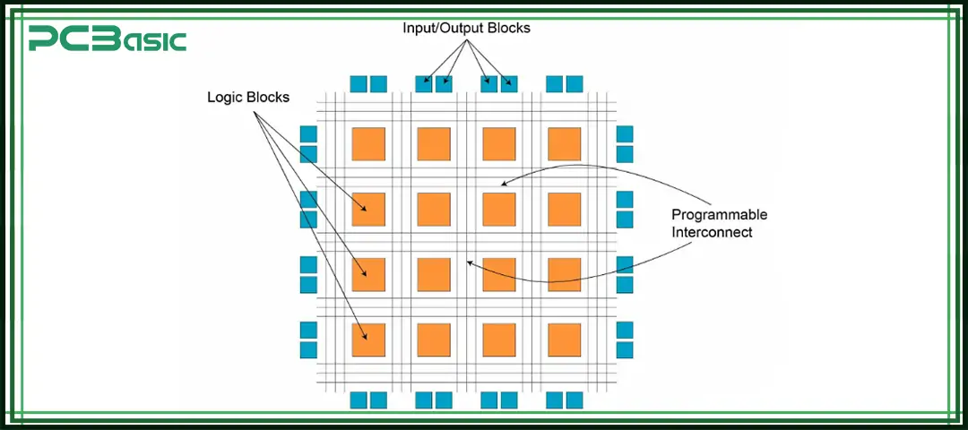
Before understanding FPGA design, we must first know what key components are inside an FPGA chip. The main components include:
• Configurable Logic Blocks (CLBs): CLBs are the core of the FPGA. They can perform various logical functions through programming and serve as the foundation for building custom circuits.
• Look-Up Tables (LUTs): Each CLB contains LUTs. LUTs can implement various logical calculations and are a key component for FPGAs to achieve flexible functions.
• Flip-Flops: They are used to store data and in FPGA design for constructing sequential circuits.
• Routing Resources: These resources are responsible for connecting CLBs and other components. Whether the routing design is reasonable directly affects the efficiency of FPGA programming.
• Input/Output Blocks (IOBs): IOBs manage data exchange between FPGA and external devices.
• Dedicated Resources: Modern FPGA chips usually also come with hardware multipliers, DSP units, block RAM, phase-locked loops (PLLs), and high-speed transceivers. These are used to support complex FPGA applications.
Mastering the functions of these basic components is essential knowledge for every FPGA engineer who wants to develop deeply in the fields of FPGA design and FPGA programming.
The FPGA design has many advantages, which make it a popular choice for all kinds of digital projects:
|
Advantage |
Description |
|
Flexibility |
Reprogrammable; functions can be changed anytime |
|
Parallel Processing |
Supports massive parallelism; faster task handling |
|
Short Time-to-Market |
Enables rapid development and faster launch |
|
Customization |
Hardware can be tailored for better performance |
|
Upgradeability |
Features can be added or fixed via software update |
|
Long Product Life |
Design can be updated; longer device lifespan |
These advantages make FPGA indispensable in the cutting-edge field and further highlight the importance of strong FPGA design and FPGA programming skills.
Although FPGA and FPGA design have many advantages, there are also some limitations:
|
Disadvantage |
Description |
|
Power Consumption |
FPGAs use more power than ASICs for the same tasks |
|
Cost |
ASICs are more cost-effective for high-volume production |
|
Speed |
FPGAs may be slower than some custom silicon |
|
Complexity |
FPGA programming requires expertise; debugging is harder |
|
Size |
FPGA chips are larger than equivalent ASICs |
Understanding these disadvantages is crucial for FPGA engineers when determining whether a project is suitable for FPGA design.
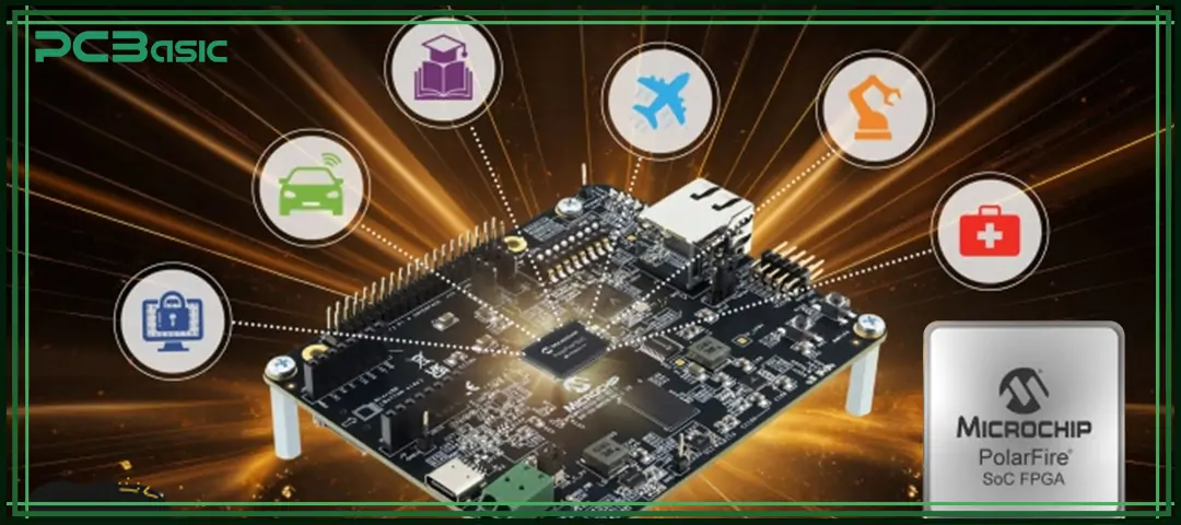
FPGA applications are very extensive, covering almost all electronics industries. Due to its high versatility and programmability, FPGA is used in various critical scenarios, including:
Telecommunications: FPGA design is used for real-time signal processing, data encryption and protocol conversion, helping communication networks improve speed and security.
Aerospace and Defense: FPGA chips are used in radar, navigation, electronic countermeasures and encrypted communication systems to adapt to complex and demanding environments.
Automotive: Advanced driver-assistance systems (ADAS), multi-sensor fusion, and in-car entertainment systems all rely on FPGA programming to achieve real-time response and high reliability.
Medical Devices: Devices such as medical imaging, automatic diagnosis, and patient monitoring enhance processing speed and detection accuracy through custom FPGA design.
Industrial Automation: The parallel processing capabilities of FPGAs are widely adopted in robots, intelligent inspection and automatic control systems to enhance production efficiency and the intelligence level of systems.
Artificial Intelligence & Machine Learning: FPGA applications achieve hardware-level efficient computing in scenarios such as neural network inference, edge computing, and big data analysis.
Consumer Electronics: Products such as high-end audio equipment, home game consoles and high-definition video accelerators usually integrate FPGA chips to enhance the multimedia experience.
It is because the field of FPGA applications is so extensive that FPGA engineers and the perfect FPGA design process have always maintained an extremely high demand throughout the electronics industry.
Time is money in your projects – and PCBasic gets it. PCBasic is a PCB assembly company that delivers fast, flawless results every time. Our comprehensive PCB assembly services include expert engineering support at every step, ensuring top quality in every board. As a leading PCB assembly manufacturer, we provide a one-stop solution that streamlines your supply chain. Partner with our advanced PCB prototype factory for quick turnarounds and superior results you can trust.
Understanding how an FPGA works is the foundation for mastering FPGA design. The FPGA is internally composed of many Configurable Logic Blocks (CLBs), and these modules are interconnected through routing resources.
When users want to implement a certain function or algorithm, they will use hardware description languages (HDL), such as VHDL or Verilog, to write the logical requirements into code. This process is called FPGA programming and is specifically divided into several steps:
Design Entry: The FPGA engineer uses HDL code to describe the required functionality.
Synthesis: The FPGA software translates the code into a circuit network.
Implementation: The circuit is assigned to the hardware resources inside the FPGA chip.
Programming: The final design is written into the FPGA, allowing it to operate as intended.
This process can be repeated many times. As long as the requirements change, the FPGA can be reprogrammed at any time. This flexibility is the greatest feature of FPGA design and also an important reason for the continuous expansion of FPGA applications.
Modern FPGA design cannot be done without various FPGA software and hardware tools. Commonly used tools include:
HDL Editors: Tools for writing VHDL or Verilog code, such as Xilinx Vivado and Intel Quartus.
Synthesis Tools: Convert HDL code into a netlist suitable for the FPGA chip.
Place-and-Route Tools: Map the logic onto the actual physical locations of the FPGA.
Simulation Tools: Check the logic of the FPGA design before loading it onto hardware.
Programmers: Write the generated bitstream into the FPGA chip.
IP Cores: Pre-designed functional modules that can be directly integrated into your FPGA design, such as memory controllers or communication protocol modules.
Mastering these FPGA software and tools is the foundation for every FPGA engineer to do well in FPGA programming and deliver FPGA applications with high quality.
The FPGA design is the standard step to turn ideas into hardware products. Every step is crucial. The specific process is as follows:
1. Specification: Firstly, it is necessary to clarify what functions the FPGA application intends to achieve and determine the performance indicators and usage environment.
2. Design Entry: Write HDL code using FPGA software to describe the logical functions in detail.
3. Simulation: Simulate HDL code on a computer to verify the correctness of the logic and identify design issues.
4. Synthesis: Use synthesis tools to convert HDL code into netlist files suitable for the target FPGA chip.
5. Implementation/Place and Route: Allocate the logic circuits to the specific resources of the FPGA, arrange the routing, and optimize the hardware layout.
6. Bitstream Generation: Generate a bitstream file for all configurations, which is used to configure the FPGA chip.
7. Programming: Use a programmer to download the bitstream file into the FPGA chip to make the hardware run.
8. Testing and Verification: Test the FPGA application on real hardware to ensure that the functionality and performance meet the standards.
9. Iteration: If problems are identified or new requirements arise, one can return to any previous step to make revisions and reprogram. The flexibility of FPGA design is reflected here.
The entire process requires an FPGA engineer who is proficient in both hardware and software. No step can be taken lightly. Because of this, FPGA programming has become a professional and highly valuable technology.
FPGA design is at the core of modern electronic technology, offering great flexibility, parallel processing capabilities, and hardware customization functions. It has been widely applied in various fields, from telecommunications and automotive systems to artificial intelligence and consumer electronics. The influence of FPGA applications is constantly expanding, driving the development of future technologies.
When you start learning FPGA design, mastering FPGA programming and getting familiar with dedicated FPGA software will help you design efficient and stable systems. Through continuous practice and understanding of the design process, you will be able to fully leverage the potential of FPGA chips and promote the innovation and development of the next generation of FPGA applications.

Assembly Enquiry
Instant Quote
Phone contact

+86-755-27218592
In addition, we've prepared a Help Center. We recommend checking it before reaching out, as your question and its answer may already be clearly explained there.
Wechat Support

In addition, we've prepared a Help Center. We recommend checking it before reaching out, as your question and its answer may already be clearly explained there.
WhatsApp Support

In addition, we've prepared a Help Center. We recommend checking it before reaching out, as your question and its answer may already be clearly explained there.