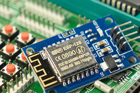
There are many pcb designers and pcb design companies that provide online pcb design services. You can also learn basic pcb design, high speed pcb design, or advanced pcb design knowledge in their online pcb design course. This easy pcb design for beginners is very suitable. So what are the important points about pcb design and manufacturing? What we are talking about is anti-interference design principles. And the anti-interference problem is a very important link in modern basic pcb design, which directly reflects the performance and reliability of the entire system. At present, the anti-jamming technologies used in the pcb design and manufacturing mainly include hardware anti-jamming technology and software anti-jamming technology.
1) The basic pcb design of hardware anti-jamming technology.
The carrier signal of the inverter circuit of the flywheel energy storage system up to 20kHz determines that it will produce noise, so that the noise and harmonic problems generated by the power electronic devices in the system become the main interference, which will affect the equipment and nearby instruments , The degree of influence is related to factors such as the anti-interference ability of its control system and equipment, wiring environment, installation distance and grounding method.
2) The basic pcb design of software anti-interference technology
In addition to taking a series of anti-jamming measures on the hardware, measures such as digital filtering, setting software traps, and using watchdog program redundancy design to make the system run stably and reliably on the software. In particular, when the energy storage flywheel is in a certain working state for a long time, the state should be continuously detected in the main loop, and the corresponding operation should be repeated, which is also a method to enhance reliability.
The anti-jamming
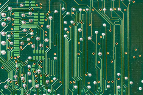
PCB layout design is closely related to the specific PCB design. Here is a collection of comprehensive and detailed PCB anti-jamming design principles to share with you.
The specific pcb design and layout principles are as follows:
1. Configuration of components
(1) Do not have too long parallel signal lines
(2) Ensure that the clock input terminals of the pcb clock generator, crystal oscillator and cpu are as close as possible, while keeping away from other low-frequency devices
(3) The components should be arranged around the core device, and the lead length should be minimized
(4) Partition layout of PCB board
(5) Consider the position and direction of the pcb board in the chassis
(6) Shorten the lead between high-frequency components
2. Configuration of decoupling capacitor
(1) Add a charge and discharge capacitor (10uf) for every 10 integrated circuits
(2) Leaded capacitors are used for low frequency, and chip capacitors are used for high frequency
(3) A 0.1uf ceramic capacitor should be arranged for each integrated chip
(4) Low noise resistance, high frequency decoupling capacitors should be added to devices with large power changes when shutting down
(5) Do not share vias between capacitors
(6) Decoupling capacitor leads should not be too long
3. The design of the power cord
(1) Choose the right power supply
(2) Widen the power cord as much as possible
(3) Ensure that the power cord, bottom line direction and data transmission direction are consistent
(4) Use anti-interference components
(5) Add decoupling capacitor (10~100uf) to the power inlet
4. Design of the ground wire
(1) Separate analog ground and digital ground
(2) Try to use single point grounding
(3) Widen the ground wire as much as possible
(4) Connect the sensitive circuit to a stable ground reference source
(5) Partition design of pcb board to separate high-bandwidth noise circuits from low-frequency circuits
(6) Minimize the area of the ground loop (the path formed by returning all devices to the ground after all devices are grounded is called "ground loop")
5. Other pcb design and layout principles
(1) The unused pins of CMOS should be connected to ground or power through resistance
(2) Use RC circuit to absorb the discharge current of relays and other original components
(3) Adding a 10k pull-up resistor on the bus helps to resist interference
(4) The use of full decoding has better anti-interference
(5) The components do not need pins to connect to the power supply through a 10k resistor
(6) The bus should be as short as possible, try to keep the same length
(7) The wiring between the two layers should be as vertical as possible
(8) Heating components avoid sensitive components
(9) Horizontal wiring on the front side and vertical wiring on the reverse side. As long as space permits, the thicker the wiring, the better (only ground wire and power wire)
(10) To have a good ground line, try to route the line from the front side, and use the back side as a ground line
(11) Keep a sufficient distance, such as the input and output of the filter, the input and output of the optocoupler, the AC power line and the weak signal line, etc.
(12) Long line plus low pass filter. The trace should be as short as possible, and the long line that must be taken should be inserted into a C, RC, or LC low-pass filter at a reasonable position
(13) Except for the ground wire, do not use thick wires if you can use thin wires