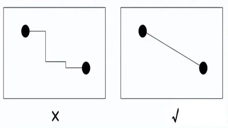
1. Length Control in Routing
Length control is a key factor in PCB design. At PCBasic, our engineers always ensure that traces are kept as short as possible to minimize potential interference caused by excessive length. For critical signal traces, such as clock or high-speed differential signals, we recommend placing the corresponding oscillator or driver very close to the target device to ensure signal integrity and stability.
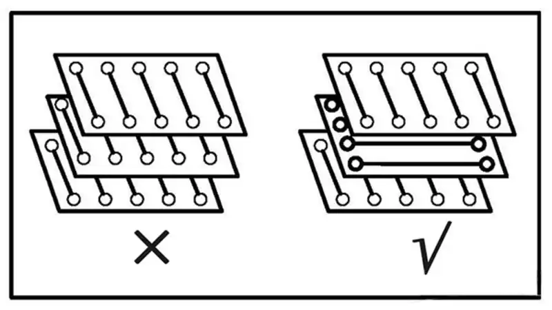
2. Direction Control in Routing
When routing multilayer PCBs, the routing direction of adjacent layers should be orthogonal to each other. This helps reduce crosstalk between signals running on adjacent layers. PCBasic’s advanced auto-routing optimization and signal integrity verification system ensure that orthogonal routing patterns are properly maintained to achieve optimal EMC performance.
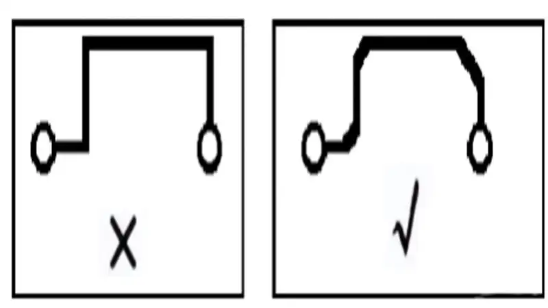
3. Rules for Chamfer
In PCB design, sharp corners and right angles should be avoided. Such structures can cause unnecessary electromagnetic radiation and lead to poor manufacturability during production. PCBasic’s DFM (Design for Manufacturability) review process automatically detects and optimizes these areas to improve both signal performance and production yield.
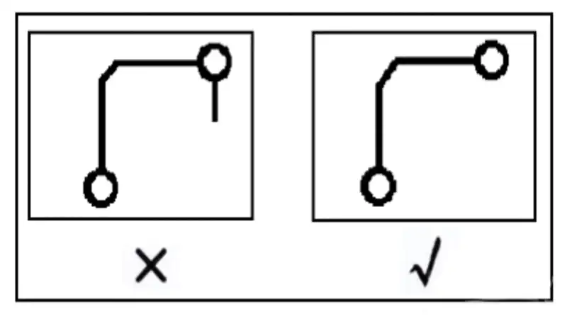
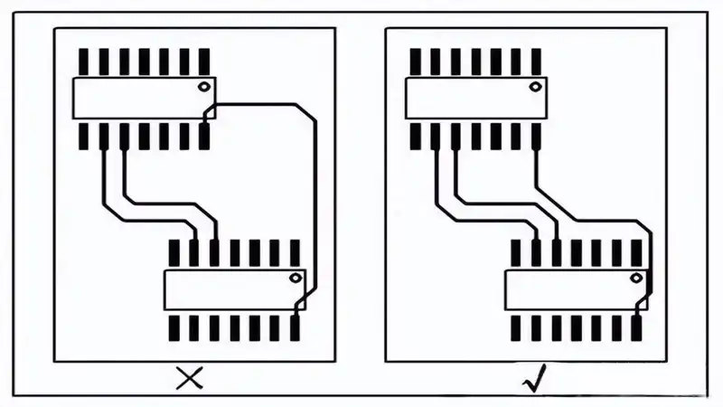
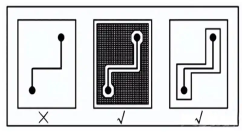
4. Open Loop Detection in Routing
Dangling or open-ended traces are generally not allowed. These can create an “antenna effect”, increasing susceptibility to EMI (electromagnetic interference). PCBasic uses ERC (Electrical Rule Check) and DFM inspection to ensure no open loops exist before manufacturing, preventing potential reliability issues.
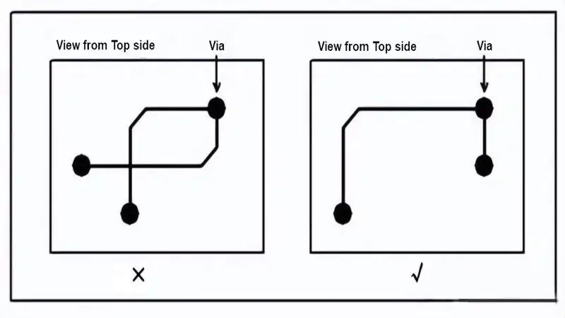
5. Try to Avoid Self-loop Routing
Designers should avoid self-looping traces across different layers. In multilayer boards, signal traces can easily form closed loops if routed incorrectly, leading to radiation interference. PCBasic’s layout verification tools can effectively detect and correct such self-loop routing problems before fabrication.
6. Rules for Ground Loop
Following the minimal loop rule, the loop area formed by a signal trace and its return path should be as small as possible. Smaller loops emit less external radiation and are less susceptible to external interference. PCBasic’s signal return path analysis ensures compact and well-controlled loop geometries.
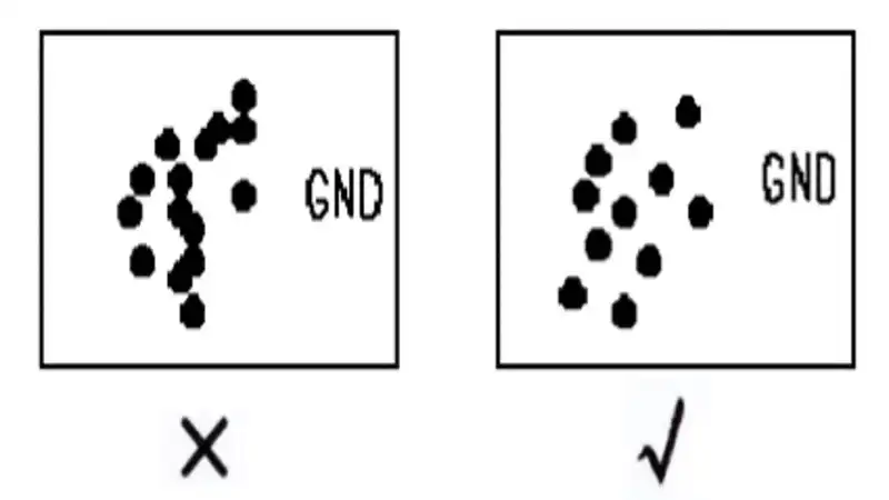
7. Rules for the Integrity of Power and Ground Layers
In areas with dense vias, attention must be paid to prevent the segmentation of power or ground planes caused by via clusters. Plane segmentation compromises the integrity of reference layers and enlarges signal loops, increasing EMI. PCBasic’s engineers apply EMI suppression design rules and ground stitching vias to maintain a solid reference plane.
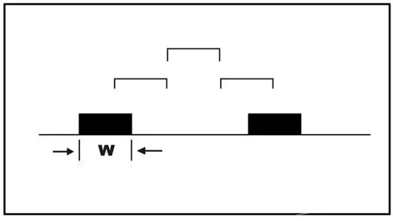
8. 3W Rule
To reduce crosstalk between signal traces, spacing must be adequate. When the center-to-center distance between adjacent traces is at least three times the trace width (3W), around 70% of the electric field will not interfere. For even better isolation—up to 98%—a 10W spacing can be used. PCBasic’s routing system automatically enforces 3W/10W rules during high-speed layout design.
9. Shielding Protection
Shielding protection helps minimize loop areas for key signals, especially high-frequency, clock, and synchronization signals. For extremely sensitive traces, PCBasic engineers adopt ground shielding or coaxial cable design, isolating signal lines with grounded copper pours on all sides (top, bottom, left, right). Proper grounding of the shield layer to the main ground plane is always ensured.
10. Rules for Impedance Matching Check
Traces within the same signal network should maintain consistent width to ensure uniform impedance. Sudden width variations can cause signal reflections in high-speed circuits. PCBasic’s impedance control routing and simulation tools help maintain uniformity. In unavoidable cases, such as connector breakout areas or BGA fanouts, the inconsistent trace sections are minimized in length.

11. Rules for Overlapping Power and Ground Layers
Different power planes should avoid overlapping in the same layer stack region to minimize coupling and interference between supplies—particularly when the voltages differ greatly. If overlap is unavoidable, PCBasic recommends inserting an intermediate ground plane for shielding.

12. 20H Principle
To suppress edge radiation, the power plane should be retracted relative to the ground plane edge. Using H (the dielectric thickness between power and ground) as a unit:
• A 20H retraction confines about 70% of the electric field within the ground plane.
• A 100H retraction confines approximately 98%.
At PCBasic, our high-speed PCB design team applies the 20H rule in stack-up design to enhance EMC performance and signal integrity, especially for RF, communication, and automotive PCBs.


