Global high-mix volume high-speed PCBA manufacturer
9:00 -18:00, Mon. - Fri. (GMT+8)
9:00 -12:00, Sat. (GMT+8)
(Except Chinese public holidays)
Global high-mix volume high-speed PCBA manufacturer
9:00 -18:00, Mon. - Fri. (GMT+8)
9:00 -12:00, Sat. (GMT+8)
(Except Chinese public holidays)
HomePage > Blog > Knowledge Base > What Are PCBs Made Of? Things You Need to Know About Printed Circuit Boards
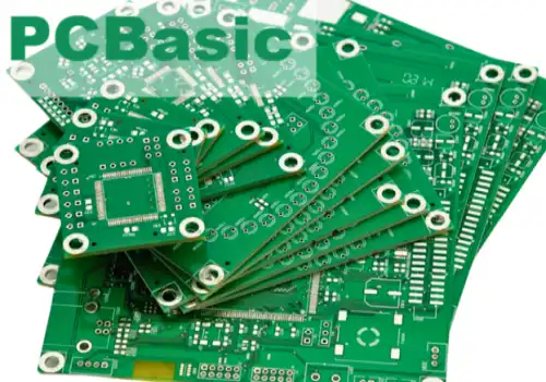
PCBs—printed circuit boards—are made from layers of materials, usually including a base layer of fiberglass or epoxy resin (providing durability), copper layers to make the circuits, and solder masks shielding the copper. They are important because they form the basis of almost all modern electronic devices, from cell phones to industrial machines. Circuit boards have been widely used by the community for a long time, but many people do not know how PCB is made and works. Let's take a look at what are PCBs made of!
Printed circuit boards (PCBs) are classified by the number of layers as single-sided, double-sided, or multilayer. Based on their substrate materials, PCBs can also be categorized as rigid, flexible, or flex-rigid.
A single-sided PCB:
comprises a protective solder mask, silkscreen, and conductive metal layer.
A double-sided PCB:
There is a conductive layer on each side.
A multilayer PCB:
is when a circuit board has more than two layers of conductive materials.
A rigid printed circuit board (PCB):
The layers of a rigid printed circuit board (PCB) — including substrate layer, copper layer, solder mask and silk screen— are pressed together with adhesive and then heated.
Flex PCBs:
consist of one or more layers of polyimide (PI) substrate, which are bonded to materials like fiberglass or metal.
Rigid-flex PCBs:
The weaved fiberglass soaks with many adhesives, epoxy resin, polyimide or polyester (PET) and copper provide the substrate material for rigid-flex PCBs.
PCB materials include insulating substrates, pads, traces, and conductive metals such as copper foil.
PCB Substrate:
PCB substrate is a key base material of circuit boards. Dielectric PCB material provides insulation, mechanical support, and electrical connectivity. Its insulating materials are generally of fiberglass or plastic.
Common substrate materials for PCBs include aluminum, polyimide, Rogers (polymer–ceramic composites), and FR-4 (fiberglass-reinforced epoxy resin). These are ceramics that can be combined with PCB materials to enhance dielectric strength.
Copper Foil
Copper foil is a crucial material used in the layers of circuit boards, with various applications around the clock. BASE COPPER refers to the copper thickness applied to both the outer and inner layers of a multilayer PCB. It is made from a 99.99% purity electrolytic grade copper cathode.

Pads and Traces
A pad is the metalized area of a circuit board layer meant to connect with the lead from a component using solder, and it can be made of PCB materials like gold, copper, or aluminum.
A circuit board trace is a conductive path molded into the substrate layer of the printed circuit board by etching, most often from copper. The traces on a printed circuit board (PCB) are vital materials to ensure signals can pass reliably between the components.
Vias
Vias are tiny holes through a printed circuit board layer that provide communication among multiple layers for electronic signal and electrical current. These vias are perforated and filled with conductive PCB materials (such as copper or silver epoxy) that electrically connect the individual layers of the board. These are very important for Multilayer Circuits.
A Solder Mask
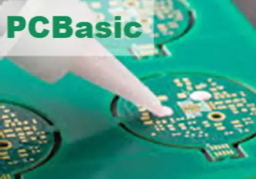
A solder mask is a thin, lacquer-like coating applied over the copper traces of a circuit board layer. This protective layer is crucial in PCB manufacturing, as it shields the copper from oxidation and prevents solder bridges between closely spaced solder pads. The solder mask, typically made from epoxy liquid or dry film, ensures the durability and reliability of the circuit board.
Silkscreen
On a PCB, silkscreen means all the ink traces created in printing on a copper board layer. Its role is to accurately locate components, measuring points, PCB sections and warning signs on the circuit board.
If you want to learn more, please click here.
The common components of Printed Circuit Boards (PCB) are transistors, resistances, capacitors, inductance and insulation.
1. Resistors — They allow an electric current to pass through, which creates a voltage and then gives off electrical energy as heat inside the printed circuit board (PCB).
2. Transistor: It is an amplifier used to regulate or switch electronic signals within a circuit assembly.
3. Capacitors: In electrical circuits, capacitors are the second most common component after resistors. They store and supply additional charges, providing extra power where needed across the board. This is typically achieved by storing opposing charges on two conductive plates separated by an insulating material.
4. Electric inductors: Inductors are capacitors that store energy, creating a magnetic field as an electric current passes through it. They are commonly used to interfere with signals inside the board and suppress interference, for example, from another electronic device or equipment.
5. Diode: This is simply a device designed to only allow current flow in one direction.
6. Conductor: A conductor is an electric pathway using traces and lands.
The PCB design process involves using CAD software to create circuit boards. The process is divided into two main stages: schematic capture (designing circuit connections in a diagram) and PCB layout (designing the physical circuit).
Key steps include:
Component Development: Creating necessary CAD components like schematic symbols, simulation models, and footprints.
Schematic Design: Populating the schematic with symbols and performing simulations to ensure electrical functionality.
Layout: Transferring connectivity data to layout tools, placing components, and routing traces while adhering to design guidelines.
Fabrication Preparation: Converting the PCB design into manufacturing drawings and checking all library components.
Final Checks: Verifying proper spacing, component alignment, and conducting final design rule checks.
Manufacturing Preparation: Completing the design, transferring files to the fabrication facility, and preparing the board for assembly.
The process concludes with the physical manufacturing of the PCB, ensuring all design elements meet the required specifications.
PCBs are an essential component of today's technology. Most printed circuit boards (PCBs) are applied to technical equipment, including consumer electronics like smartphones, smartwatches, computers, televisions, and other devices. The industrial sector can also utilize PCBs, such as assembly machines, electrical equipment like power supplies and inverters, and temperature measurement devices. Printed circuit boards (PCBs) also extend to medical equipment, including X-ray displays, blood glucose monitors, and other similar devices.
PCBasic was established in 2011 and is located in Shenzhen, China. PCBasic has been working in PCB/PCBA manufacturing for nearly a decade and achieved pioneering breakthroughs.
With outstanding expertise in printed circuit boards and decades of work experience, PCB Machine is confident enough to get through any technical challenges and bring the best materials for PBCs & PCBA as a prominent PCB maker worldwide. Assign your PCB designs to PCBasic Today!
To find out more on PCBasics, please go to www.pcbasics.com.
Printed circuit boards (PCBs) are complex assemblies with many essential components that ensure their functionality and durability. For a PCB to work properly, each component must perform its role effectively. Therefore, careful attention is needed throughout the design process to ensure all elements function together seamlessly.
Assembly Enquiry
Instant Quote
Phone contact

+86-755-27218592
In addition, we've prepared a Help Center. We recommend checking it before reaching out, as your question and its answer may already be clearly explained there.
Wechat Support

In addition, we've prepared a Help Center. We recommend checking it before reaching out, as your question and its answer may already be clearly explained there.
WhatsApp Support

In addition, we've prepared a Help Center. We recommend checking it before reaching out, as your question and its answer may already be clearly explained there.