Global high-mix volume high-speed PCBA manufacturer
9:00 -18:00, Mon. - Fri. (GMT+8)
9:00 -12:00, Sat. (GMT+8)
(Except Chinese public holidays)
Global high-mix volume high-speed PCBA manufacturer
9:00 -18:00, Mon. - Fri. (GMT+8)
9:00 -12:00, Sat. (GMT+8)
(Except Chinese public holidays)
HomePage > Blog > Knowledge Base > Signal Integrity in PCB Design: Analysis, Testing, and Simulation
In modern high-speed electronic devices, signal integrity has become an issue that hardware engineers must pay attention to. As PCBs become smaller and signal speeds increase, even the slightest routing error, impedance mismatch or unreasonable via design can lead to signal distortion, timing issues, or even equipment failure to operate properly.
In PCB design, signal integrity determines whether the signal can still maintain the correct waveform during transmission and be accurately identified by the receiver. Common influencing factors include transmission line effects, crosstalk, impedance mismatch and ground bounce. If these problems are not well controlled in the early design stage, the product may fail in the electromagnetic compatibility test (EMC) or malfunction in actual use.
To avoid these risks, engineers need to conduct signal integrity analysis in the early design phase, use simulation tools to predict potential issues and verify the reliability of the design through signal integrity testing and signal integrity measurements.
This article will introduce you to the signal integrity basics, analyze common signal problems in PCBs, and explain the mainstream signal integrity simulation and testing techniques. And recommend practical signal integrity tools and signal integrity solutions to help you enhance the overall signal and power integrity. Make the electronic system more high-speed, stable and reliable.

Understanding the basics of signal integrity is the first step in doing a good job in high-speed circuit design. Simply speaking, signal integrity refers to whether a signal can maintain its original shape and timing when traveling across the circuit board. If the signal is distorted, weakened or delayed during transmission, it may cause the device to misinterpret a "0" or "1" (or vice versa), thereby resulting in system errors or even total failure.
In PCBs, several key issues affecting PCB signal integrity include:
Amplitude distortion: The voltage level of the signal may drop due to the resistance or capacitance or experience overshoot and undershoot, resulting in an irregular waveform.
• Timing issues: The signal may be transmitted too fast or too slow, resulting in delay, jitter or skew, disrupting the original synchronization and causing data errors.
• Signal reflection and ringing: When a signal moves between areas of different impedances, it reflects back and forth along the line, distorting the waveform.
• Noise and crosstalk: Adjacent signal lines can interfere with each other, causing original signals to be "polluted", which is particularly common when high-speed signals are densely laid out.
To master the basics of signal integrity, engineers must understand:
• How signals travel through a transmission line
• How return current completes the loop via the return path
• How PCB materials, trace width, layer structure, vias, and routing style all impact signal quality
Meanwhile, don’t only focus on the signal itself but also take into account the signal and power integrity. Unstable power (such as power noise or voltage drop) can also interfere with high-speed signals, causing abnormal system operation.
Therefore, from the first step of the design, signal integrity simulation and signal integrity analysis should be combined to optimize the layout and routing, reducing the risk of failure in signal integrity testing in the later stage. Using the right signal integrity tools and signal integrity solutions is the key to building stable operation of high-speed PCBs.
There are many factors affecting signal integrity in PCB design. The following are several of the most crucial issues that engineers must pay attention to during the design process:

Transmission Lines
In high-speed PCB design, traces work like transmission lines, not just simple wires. Their shape and the materials around them affect how fast and clean signals move. If traces are too long, too thin, or not designed well, signals can lose strength or get distorted. This hurts signal integrity.
Impedance Matching and Termination Resistors
A big cause of signal integrity problems is impedance mismatch. When a signal meets a section with a different impedance, it reflects back, causing ringing. This reflection distorts the signal. Adding resistors at the right places (called termination) can absorb these reflections and improve PCB signal integrity.
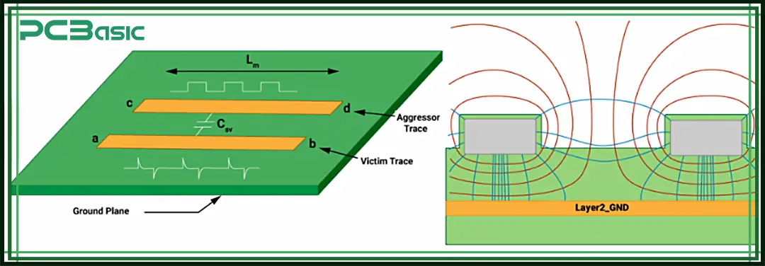
Crosstalk and Coupling
Traces that are too close can interfere with each other. This is called crosstalk. It happens because of electrical interaction between nearby traces. It's common in parallel buses and differential pairs. To reduce crosstalk and improve signal and power integrity, keep traces apart, use ground shielding, and route signals carefully.
Vias and Layer Transitions
Every via adds a small break or change in the signal path. If vias are too long or not placed correctly, they can change impedance and disrupt return paths. This causes signal distortion. Use shorter vias, good return paths, or backdrilling to protect signal integrity.
Differential Pairs
Differential signals work in pairs and resist noise well. But if the two traces in a pair are not equal in length or spacing, some of the signal can become common-mode noise. This reduces signal integrity and affects EMC performance. Keep differential pairs matched in length and spacing to avoid this.
By watching out for these common problems and following good design practices, you can greatly improve signal integrity and build more reliable high-speed PCBs.
Signal integrity analysis and simulation is a very important step in PCB design. Before making a circuit board, engineers use simulation tools to check if signals might have problems during transmission — like signal reflections, interference from nearby wires (crosstalk), or changes in impedance. Finding these issues early helps improve PCB signal integrity and avoids expensive rework later.
Signal integrity simulation lets engineers check how clean and stable the signal will be as it moves through the PCB. Here are some common simulation methods:
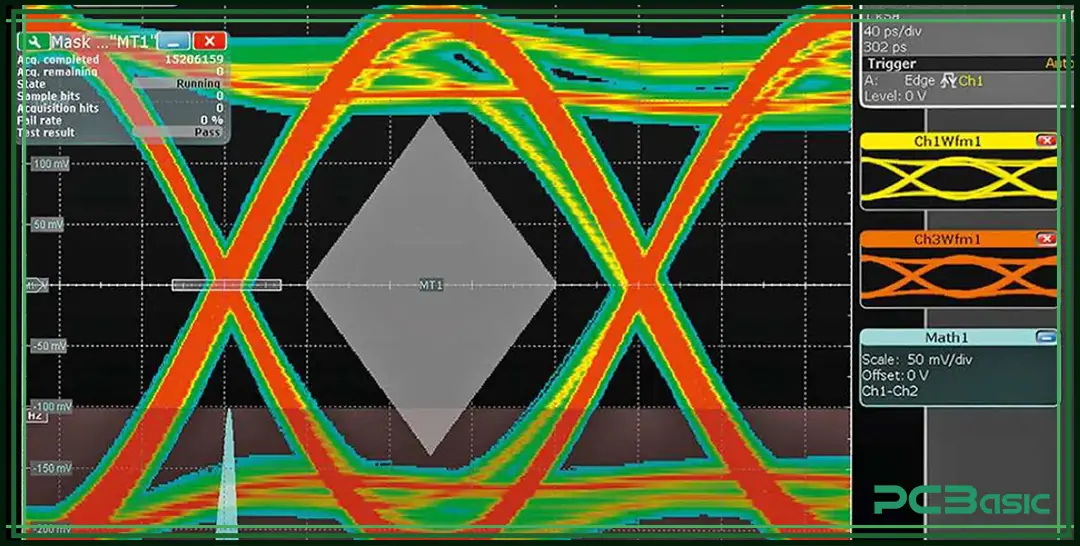
• Eye diagram analysis: This shows how stable and clear a high-speed signal is. A wide and open “eye” means the signal is clean and less likely to have errors.
• TDR (Time Domain Reflectometry): This checks for any sudden changes in impedance along the signal path, like those caused by vias or connectors. These changes can reflect signals and cause problems.
• S-parameter simulation: Often used for high-frequency designs. It shows how much of the signal gets through, how much reflects back, and how much power is lost.
• Crosstalk analysis: This checks whether signals from nearby traces are interfering with each other, which could lead to noise and data errors.
These simulations help ensure your trace layout is correct, the impedance is controlled, and there are no big design mistakes. Popular signal integrity tools that can do these simulations include Ansys SIwave, Keysight ADS, HyperLynx, and Altium Designer. These tools support both early-stage (before layout) and final-stage (after layout) checks, helping engineers make sure their designs meet all signal and power integrity standards.
 About PCBasic
Time is money in your projects – and PCBasic gets it. PCBasic is a PCB assembly company that delivers fast, flawless results every time. Our comprehensive PCB assembly services include expert engineering support at every step, ensuring top quality in every board. As a leading PCB assembly manufacturer, we provide a one-stop solution that streamlines your supply chain. Partner with our advanced PCB prototype factory for quick turnarounds and superior results you can trust.
Signal integrity testing and measurements are a very important step after PCB manufacturing. Even though we use simulations during the design stage to predict signal behavior, only real-world testing can confirm whether the signal performance on the actual board meets expectations. Signal integrity measurements help compare real signals with simulation results and verify the reliability of the design.
Common signal integrity testing methods include:
This test shows overlapping waveforms of high-speed signals over many cycles. It helps check signal stability, jitter, and timing margins. A clear eye diagram with a wide eye opening means better signal quality.
This test sends and receives high-speed data streams and measures how many bits were received incorrectly. It helps determine if the signal integrity meets the required standards.
This test checks how much the signal edges shift over time. It is useful for finding timing problems caused by interference, crosstalk, or power noise.
This test evaluates impedance matching and transmission loss. It is especially useful for high-frequency signal testing.
These test methods help engineers confirm whether the system meets timing, voltage, and signal quality requirements. They also provide feedback to improve simulation models and make signal integrity simulation results more accurate and closer to real-world performance.
Improving signal and power integrity requires optimization from both the overall system architecture and detailed PCB layout. It's not just about signal quality—it also affects the stability and reliability of the entire electronic system. Here are some clear and practical design strategies:
Each signal trace should have a continuous, low-impedance return path. This is usually done by placing a solid ground or power plane directly under the signal layer. It helps reduce loop area, minimize electromagnetic interference, and improve overall signal integrity.
Choose the right PCB layer structure and control trace width, spacing, and layer distance to maintain consistent impedance. This reduces signal reflections and ringing, helping to keep your PCB signal integrity stable.
Vias can disrupt signal paths and cause impedance changes. For high-speed signals, try to reduce the number of vias or use backdrilling to remove unused via stubs and avoid signal reflections.
Keep noisy circuits like switching power supplies away from sensitive analog or high-speed digital circuits. This prevents crosstalk and power noise from affecting signal quality, which is key to maintaining signal and power integrity.
Decoupling capacitors help filter out power noise and reduce voltage ripple. Place multiple capacitors with different values close to each power pin to handle different noise frequencies and ensure clean power delivery.
In short, a well-designed power delivery network helps improve signal integrity, while proper routing and termination strategies improve the reliability of high-speed data transmission. Both are essential for building a stable, high-performance electronic system.
Whether you're designing a high-speed microcontroller board or a complex server backplane, signal integrity is a key factor in ensuring your device runs reliably. From understanding the basic concepts to performing advanced signal integrity analysis, simulation, and testing, every step helps you create more accurate and dependable designs.
By using professional signal integrity tools and applying proven signal and power integrity techniques, engineers can catch issues early, reduce trial and error, avoid costly redesigns, and bring high-frequency products to market faster.
In simple terms, investing in strong signal integrity solutions gives your electronic products a solid foundation, helping them perform more reliably in high-performance applications.

Assembly Enquiry
Instant Quote
Phone contact

+86-755-27218592
In addition, we've prepared a Help Center. We recommend checking it before reaching out, as your question and its answer may already be clearly explained there.
Wechat Support

In addition, we've prepared a Help Center. We recommend checking it before reaching out, as your question and its answer may already be clearly explained there.
WhatsApp Support

In addition, we've prepared a Help Center. We recommend checking it before reaching out, as your question and its answer may already be clearly explained there.