Global high-mix volume high-speed PCBA manufacturer
9:00 -18:00, Mon. - Fri. (GMT+8)
9:00 -12:00, Sat. (GMT+8)
(Except Chinese public holidays)
Global high-mix volume high-speed PCBA manufacturer
9:00 -18:00, Mon. - Fri. (GMT+8)
9:00 -12:00, Sat. (GMT+8)
(Except Chinese public holidays)
HomePage > Blog > Knowledge Base > Understanding PCB Copper Thickness and Copper Weight
Current passes through printed circuit boards along their copper layers. Therefore, when you begin your stack-ups, you should focus on PCB dielectric thickness or board thickness and PCB copper thickness also. In this article, you will get to know why it is an important point.
Choosing the wrong material thickness can significantly impact circuit performance. However, understanding the relationship between copper weight and signal transmission is essential.
If you are considering designs outside of standard values, keep reading this article. This information will provide insight into the pcb thickness and its importance.
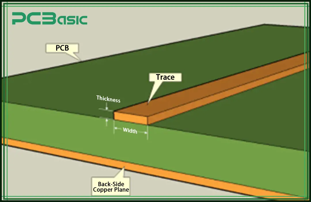
Manufacturers employ a standard thickness of copper material, usually 0.5 oz/sq ft or 1.0 oz/sq ft, in PCB production. This copper weight to thickness is generally referred to as ounces.
Copper weight is measured by the weight of copper evenly spread over one square foot. The final result of the copper foil thickness will be 1.37 mil or 0.0348 mm.
Metalworkers generally produce copper thickness of around 1 oz. However, this thickness can be substituted depending on the project requirements.
While 1 oz copper thickness is often sufficient for PCB production, increasing it can complicate the fabrication process and increase production costs and time. However, engineers often prefer to increase the width of copper traces, as this improves electrical conductivity.
1. 0.5 oz copper thickness
2. 1 oz copper thickness
3. 2 oz copper thickness
4. 20 oz copper thickness
0.5 oz copper thickness is typically used for internal layers in PCBs and is considered a non-standard construction. Manufacturers apply this thickness upon request. It can also be used as a starting copper weight for PCBs aiming for a 1-ounce finished copper weight, particularly for inner layers.
1 oz copper thickness is the standard internal layer for most PCB designs. It is suitable for achieving finished copper weights of 1-2 oz. Similarly, it's the standard starting copper weight for external layers aiming for a 2 oz finished copper weight.
2 oz copper thickness is a standard internal layer, often used for internal layers in PCBs with a finished 3 oz copper weight. Furthermore, 2 oz copper thickness is also a common starting thickness for the outer layers of PCB boards.
Copper Thickness and Weight Conversion for PCBs:
|
Copper Weight (oz/ft²) |
Copper Thickness (µm) |
Copper Mass (g/m²) |
|
0.5 oz/ft² |
17.5 µm |
152 g/m² |
|
1 oz/ft² |
35 µm |
305 g/m² |
|
2 oz/ft² |
70 µm |
610 g/m² |
|
3 oz/ft² |
105 µm |
915 g/m² |
Conversion coefficients:
· 1 ounces = 28.35 g
· 1 ft = 30.48 cm
· 1 ft² = 0.093 m² = 930 cm²
· Copper Density = 8.9 g/cm³
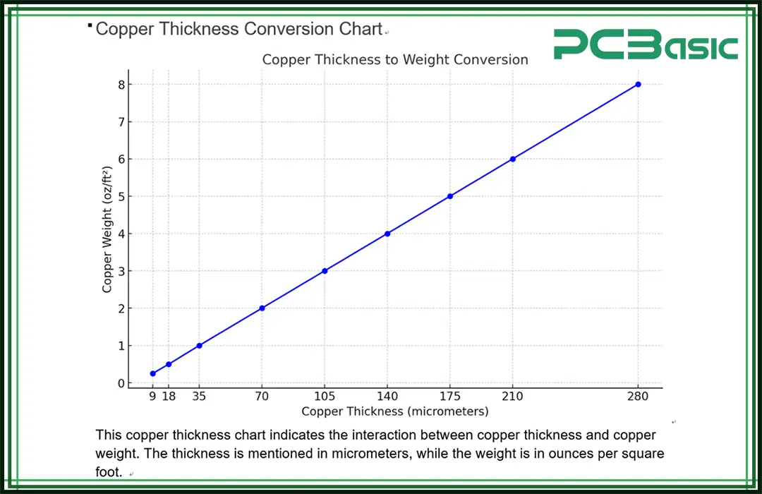
Manufacturers can commonly substitute the copper thickness beside the dimensions of printed circuit boards. Copper weight drastically can induce changes in other traits of boards.
The thickness of copper traces or their layers contributes to weighing the current-carrying capacity of PCBs. That can be somewhat determined by learning the thickness properties of copper.
Additionally, the width of copper traces is pivotal. This helps determine the suitability of copper thickness for impedance-controlled boards.
Additionally, stack-up considerations include PCB weight, connector types, and segment compatibility.

Usually, 1 oz copper thickness to 3 oz copper is employed in the assembly of PCB boards. Although, there is no suitable definition for heavy copper.
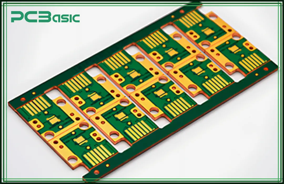
Normally, the heavy copper ranges from 2 oz copper thickness to 20 oz copper thickness. Likewise, the intense ones range from 24 oz to 200 oz. Manufacturers use heavy copper for the following reasons:
To create compact products by placing multiple copper weights on the same layers. To support larger current-carrying applications.
PCB layers are often produced with varying copper thicknesses. In the case of the underlying layers, they utilize 1 oz copper thickness. Similarly, 4 oz/sq ft copper is used for the outer layers.
During the operation stage, PCB can generate excessive heat that can bend or damage the PCB board. Manufacturers can reduce this risk. They employ the same copper weight in opposing layers.
Copper thickness enables the boards to resist frequent exposure to undue current flow. They ensure safety even under recurring thermal cycling.
Moreover, heavy copper boards can withstand applications in critical situations. They are advantageous for producing outcomes for the aerospace and defense divisions.
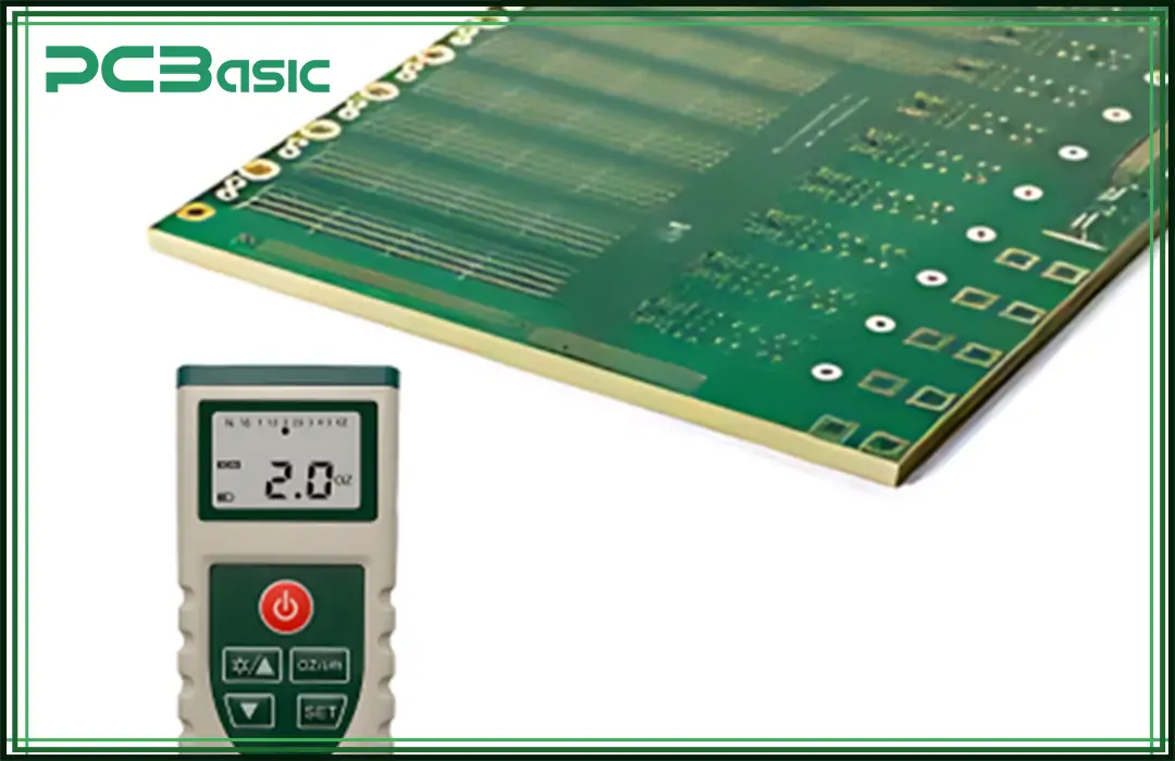
Several techniques can effectively measure copper trace thickness. Operators can choose methods suitable for their stack-ups.
A micrometer is widely operated to gauge the stratification of copper material. It is feasible to situate the copper on the surface. Place the metal in the interstice of its anvil and spindle. Then, the meter will compute the copper thickness of the film and show the exact reading.
A caliper is another way to measure copper thickness. Ensure the reading is zero. Then, place the copper and measure its thickness at several points for accuracy.
The ultrasonic gauges are subject to calculating the identical thickness of copper. Operators can choose methods suitable for their stack-ups. In this technique, the waves travel through the material surface and figure out the copper thickness. It counts the time that it takes for the waves to return.
This technique supports determining the copper weight. These X-ray sources excite the material. They measure the rays transmitted from the substances.
This technology measures conductive coatings over copper. It induces the eddy currents in the material that contributes to gauging the substance's thickness.
The weight measurement application is also an effective way to occupy the thickness calculation. This application can be deployed to measure large areas that integrate a density of copper of around 8.96 g/cm2.
Techniques like interferometry are optimal for measuring the thin layers of copper thickness. They generate light interference patterns on the surfaces. It provides accurate thickness measurement.
· Higher Minimum Track Spacing requirements
· Via Size Considerations
· The greater thickness of the solder mask
Increasing copper thickness requires greater spacing between copper features.
Track spacing is important for all copper weights. This step aims to reduce the chances of signal degradation and overheating.
Integrated circuits are usually produced of heavy copper. These are subject to handling higher-current transmission. Therefore, ensure the vias can carry the required current ratio. It should eliminate the excess resistive losses.
In conjunction, the larger vias control lower impedance paths for the flow of electric charge. They reduce the resistive heating and minimize the voltage drops.
Therefore, appraise the design choice founded on the vias that can effectively carry the higher current loads. It can maintain steadfast connections, depending on the different layers of the PCB.
Solder masks may have difficulty adhering to heavy copper due to its higher surface tension.
Improper solder mask adhesion can cause it to peel from the PCB. This results in exposed copper. This could precipitate the shorts, corrosion, and other inevitable issues.
You can amplify the solder mask thickness to avoid these predicaments. That will equip more surface area for the solder mask molecules to adhere to.

Trace width, signal transmission, and voltage drop are crucial factors when calculating copper weight. Opt for thicker copper weight if your boards are carrying a high current. This will ensure your copper traces do not produce excessive heat.
Accordingly, the thinner copper weight should be implemented to reduce the inductance of the layers. This will cater to maintaining the attribute of high signal integrity.
Additionally, heavy copper weights are sought for their ability to handle high current loads. They comprise a thickness range from 3 oz to above. It confers noteworthy thermal management.
The copper thickness is as important a factor as its other parameters while weighing the material for your project requirements. It is gauged in ounces. Changes in copper thickness chart can disrupt the performance of electronic circuit assemblies during operation. Varying copper thicknesses can be effectively implemented on the same PCB surface. However, several factors must be considered during implementation.

Assembly Enquiry
Instant Quote
Phone contact

+86-755-27218592
In addition, we've prepared a Help Center. We recommend checking it before reaching out, as your question and its answer may already be clearly explained there.
Wechat Support

In addition, we've prepared a Help Center. We recommend checking it before reaching out, as your question and its answer may already be clearly explained there.
WhatsApp Support

In addition, we've prepared a Help Center. We recommend checking it before reaching out, as your question and its answer may already be clearly explained there.