Printed circuit boards (PCBs) serve as the backbone of electronics, interconnecting components to create functional circuits.
One of the most vital PCB design elements enabling this is the pads - metallic landing areas that provide the interface between board traces and component leads. Pads must be tailored in size, shape, and layout to suit the specific parts being mounted.
Getting the pad design right is crucial for creating a working PCB assembly. This comprehensive guide aims to provide PCB designers and engineers with an in-depth understanding of pad construction, properties, and design factors.
So, here is a glimpse of what we'll be discussing over the next few minutes:
● Types of PCB Pads
● How to Put a Via on a Pad
● What is a Bond Pad
● Considerations During PCB Pad Design
● Standards and Calculators for PCB Pad Sizing
● Problems Caused by Wrong Pad Design
Yes, we'll walk through all of that and then answer some questions we've been asked as experts on PCB pad design. So, with that out of the way, let's get into the crux of the topic.
What is PCB Pad in Electronics
A printed circuit board (PCB) pad is a flat, metal-plated area on the board used to mount and connect electronic components. Pads serve as the interface between the component leads and the copper traces on them. When a part like a resistor or integrated circuit is soldered to the board, its leads are physically and electrically joined to the pads.
They come in a variety of shapes and sizes tailored to the type of component being mounted. For example, a surface mount chip resistor may have small, rectangular pads, while a through-hole electrolytic capacitor uses larger annular rings. The pad size must match the part's lead or termination style to ensure a solid joint.
PCB pads anchor the component in place mechanically while allowing current flow between the part and the adjoining circuit traces. Their layout and positioning on the board enable efficient routing to connect the attached components as intended in the circuit schematic.
Well-designed pads are essential for assembling a functioning PCB. With proper pads, components could be reliably mounted and wired into the circuit architecture.
So, these pads actually provide the crucial attachment points bridging components and board traces. Their design strongly influences manufacturability, connectivity, and, of course, their overall PCB performance.
 About PCBasic
Time is money in your projects – and PCBasic gets it. PCBasic is a PCB assembly company that delivers fast, flawless results every time. Our comprehensive PCB assembly services include expert engineering support at every step, ensuring top quality in every board. As a leading PCB assembly manufacturer, we provide a one-stop solution that streamlines your supply chain. Partner with our advanced PCB prototype factory for quick turnarounds and superior results you can trust.
Types of PCB Pads
We trust that you now have a solid grasp of the fundamentals of PCB pads and their essential functions. However, we will delve deeper by examining the various types of PCB pads in more detail.
Through-hole Pad
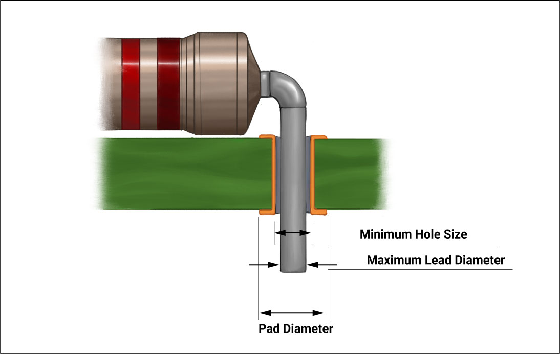
Through-hole PCB pads are designed to accommodate leaded components with wire leads that pass through holes drilled in the board. The pad itself is a round annulus surrounding the plated-through hole.
When viewed from above on the PCB surface, it appears as a ring with a hole in the center. The inner diameter of the ring matches the drilled hole size, while the outer diameter provides sufficient annular ring area for soldering the component lead.
During assembly, the component lead passes through the hole and extends out to the opposite side of the board. The lead is then clinched or soldered to form a solid mechanical and electrical connection. The plated barrel of the hole connects the pads on both sides, enabling conduction between board layers.
Through-hole pads come in varying sizes based on factors like lead diameter, solder flow requirements, and desired bonding strength. For example, a TO-220 power transistor may use large 0.4" diameter pads, while a resistor could have 0.1" pads.
Their ring shape allows generous solder fillets to form for reliability. This has been continually used for connectors, large transformers, and other components unsuited to surface mounting.
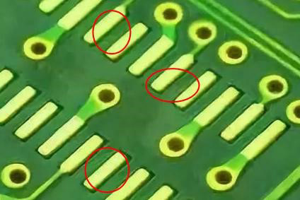
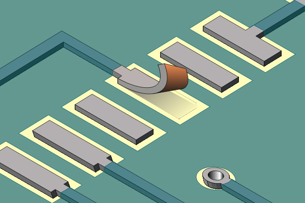
Surface Mount Pad
These are pads designed to accommodate integrated circuits and components with leads or terminations that do not pass through holes in the board. Instead, the pads provide flat surfaces to solder the part directly atop the PCB.
Common surface mount pad geometries include rectangles, circles, and rounded rectangles. The shape and dimensions match the component's lead or ball configuration.
For example, a SOIC integrated circuit package may have small rectangular pads matching the J-lead footer pattern. In comparison, ceramic capacitors and resistors use larger rectangular or square pads compatible with their end terminations. The pads are precisely located on the PCB to align with the component's lead positions when mounted.
During assembly, solder paste is applied to the pads before the part is placed. Reflow soldering forms reliable joints without leads passing through holes. Edge-mounted pads can also be used with grooves in the board to improve solder bonding further.
Well-designed surface mount pads enable high component density, automated assembly, and miniature PCB electronics.
Surface mount pads act as solderable shelves on the board to attach flat-leaded components directly. Their size, shape, and layout match the specific component terminations.
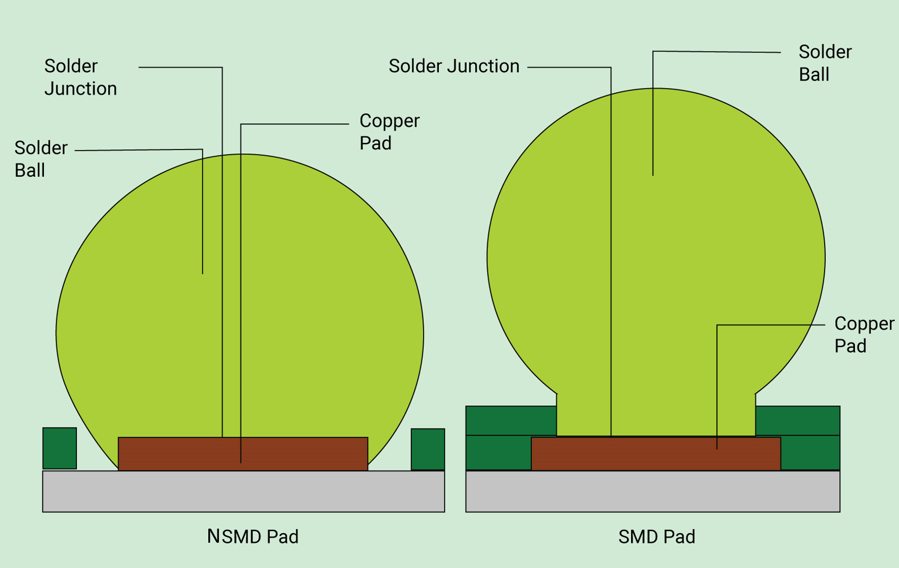
BGA Pads
BGA or ball grid array pads, as we all know them, are mounted integrated circuit packages with solder ball terminations on the underside. The pad layout mirrors the footprint of the BGA package, containing an array of small circular landing pads.
Common pitches or spacings between pads range from 0.8mm to 1.27mm. The pad diameter is slightly larger than the ball diameter to allow inspection and account for tolerances.
During assembly, solder paste is printed or deposited on the BGA pads. The IC package balls are precisely aligned and placed onto the pads. Reflow soldering forms the interconnections. The bottom side array mounting provides numerous input/output connections without requiring space-consuming edges or perimeter leads.
BGA pad layouts are optimized to match the particular package footprint being used. Factors considered include ball quantity, pitch, ball diameter, and optimal bonding area.
Signal integrity simulations help verify pad layouts before finalizing the PCB design. Correct BGA pad design is crucial for achieving reliable, high-density mounting of complex ICs like processors and FPGAs.
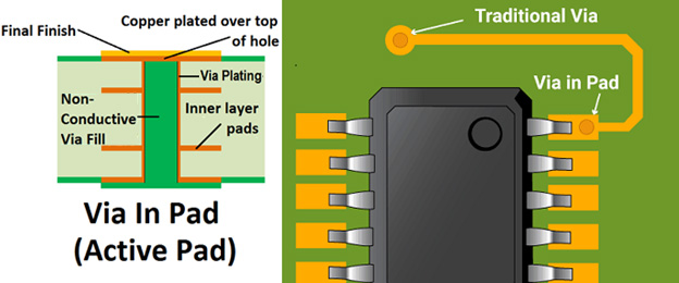
How to Put a Via on a Pad
When designing a printed circuit board (PCB), one of the key techniques you'll need to understand is how to place a via on a pad effectively. This process is crucial for creating multilayer boards, where electrical connections must pass through different layers.
A via is a small hole in the PCB that is plated or filled with metal, allowing electrical connection between different layers of the board. Placing a via on a pad, often used for component leads or mounting holes, requires precision and a good understanding of your circuit design software.
Let's delve into the specifics and steps of how this is done to ensure your PCB functions as intended.
Step 1: Deposit and Pattern the Bond Pad Material
The first step is to deposit the bond pad metal, typically aluminum or copper, onto the topmost metal layer of the integrated circuit using methods like sputtering or evaporation. Photolithography transfers a pattern onto a photoresist layer to define bond pad layout. The exposed areas are etched away, leaving the required pad geometries.
Step 2: Deposit the Dielectric Layer
Next, a dielectric insulation material like silicon dioxide or nitride is deposited over the entire wafer surface using chemical vapor deposition. This electrically isolates the conductive pads. The dielectric thickness depends on the via height needed.
Step 3: Pattern Via Photoresist
A new photoresist layer is placed and patterned with the via locations aligned over the bond pads. The resist is exposed and developed, revealing these via sites while keeping the rest of the dielectric covered.
Step 4: Etch Via Holes
Now, using the patterned photoresist as an etch mask, the dielectric is etched away by reactive ion etching. This anisotropic etch forms vertical sidewalls, stopping when the underlying bond pad is reached. Etch depth is precisely controlled to avoid over-etching into the pad.
Step 5: Strip Photoresist
After via etching, the remaining photoresist is stripped away using solvents or O2 plasma ashing. A short step cleans out any polymer residues from via holes.
Step 6: Deposit Via Metal
The vias are filled using highly conductive metals such as tungsten or copper and deposited into the holes by methods like CVD or electroplating. This establishes electrical connectivity down to the bond pad.
Step 7: Planarize the Surface
Chemical mechanical polishing (CMP) is used to planarize and smooth the wafer surface via metal deposition. The CMP slurry contains chemical etchants and mechanical abrasives that remove excess metal and dielectric. The rotating polishing pad presses against the wafer to physically grind away protrusions. This continues until a flat surface is achieved, isolating the individual vias. The metal remaining in the etched holes provides the electrical connection down to the bond pads.
Step 8: Final Inspection
Multiple inspection techniques verify the pad via integrity after CMP planarization. Optical microscopy with high magnification mode checks for potential defects like residual scratches, particles, or holes in the via metal. Scanning electron microscopy provides even higher-resolution imaging. Electrical probing tests for opens and shorts between vias by forcing a current and measuring resistance. This screening ensures each via achieves robust connectivity to its underlying bond pad.
Step 9: Deposit the Next Layer
With the bond pad vias completed, fabrication continues by depositing the next dielectric and metal layers. This adds more metallization levels, building upward from the silicon transistors and interconnects toward the pad interfaces. Dielectrics are electrically separate conductive traces, while vias provide vertical connections between layers. The integrated circuitry becomes progressively more dense, approaching the pads. The final structure enables signals to route across the chip into the pads, connecting through the now-formed vias.
What is a Bond Pad
Bond pads are conductive areas on a semiconductor die or chip providing connection points to attach fine bonding wires.
They allow electrical signals and power to be transmitted on and off the integrated circuit. Bond pads are generally made of aluminum or copper and plated with gold or other metals to enable wire bonding and prevent oxidation.
The pads are positioned along the periphery of the die surface, with the exact number, spacing, and layout dependent on the chip's input/output requirements.
A complex processor may have hundreds of tiny bond pads, while an LED chip may only need a few larger pads. The interface through microscopic gold or copper wires is just 15-35 microns thick and attached using thermal-sonic or ultrasonic bonding.
Bond wires then connect the pads to external pins or leads of the IC package. This enables signal fan-out to board-level interconnections. Proper pad material, size, and layout ensure reliable bonding connections and electrical performance.
Bond pads are a crucial interface enabling chips to be packaged and deployed in electronic systems. They facilitate communication despite the extremely small scale of semiconductor devices. With high-density pad arrangements, large amounts of data can be input and output using the tiny bonding wires interfaced to the IC.
What Should Be Considered During PCB Pad Design
Thoughtful pad design is imperative to ensure reliable component mounting and interconnections on a printed circuit board.
Engineers must weigh numerous factors when planning pad geometries and layouts tailored to their specific application and selected components.
So, below are key things that must be considered during PCB pad design.
Component Type and Termination Style
The pad must match the physical interface of the component being mounted. Different part types, like resistors, capacitors, ICs, connectors, etc., have varying terminal configurations.
For example, an axial leaded resistor needs a round pad with a hole, while a surface mount chip capacitor utilizes rectangular pads.
The size, shape, pitch, and layout of pads must align with the leads or pads on the component footprint. This ensures the solderable contact areas correctly match the part. Designers must tailor pad geometry to the termination style.
Mounting Technology
Factors like through-hole versus surface mount, soldering method, press-fit, or other assembly processes influence pad design.
Pads for wave soldering may require extended terminals and thermal relief spokes. Reflow soldering needs an opening in the solder mask for paste application. Press-fit parts are plated through holes with copper protrusions.
Beyond soldering, factors like adhesive bonding, welding, or sockets determine appropriate pad specifications. The pad interface must suit the intended mounting technique.
Mechanical Stability
Pads anchor components against stresses like shock, vibration, and temperature swings. Adequate pad size and number of joints improve mechanical robustness. Large pads or additional anchor pads can be used for big, heavy parts.
Thermal relief cutouts in pads reduce cracking from CTE mismatch between board and parts. Other pad shapes improve solder joint integrity. Mechanical analysis helps determine suitable pad features for robust mounting.
Electrical Connectivity
Low-inductance, high-current pads may utilize thicker copper or thermal planes for power devices. Signal pads require controlled impedance connections to traces. Ground pads need sufficient ampacity for return currents.
Split reference planes necessitate isolation between pad zones. Parasitic effects must be minimized. Pad design aims for optimal electrical performance given the component function and circuit architecture.
Thermal Management
Pads conduct heat from components into the board, so sufficient pad area should be provided for cooling. Large copper pads or thermal planes help spread heat.
Thermal reliefs reduce conduction through solder joints, preventing hot spots. Heat sinks may be used for high-power parts. Thermal analysis informs pad size and layout to maintain safe component temperatures.
Manufacturability
Pads must enable cost-effective board fabrication. Plating thickness, drill tolerances, lamination temperatures, and other factors constrain pad geometries. Non-circular pads increase drilling time and tool wear.
Small pads hinder solder mask alignment. Close pad spacing reduces solder bridging risks but complicates fabrication. Design for Manufacturing (DFM) practices ensure pads can be reliably produced.
Routing Constraints
Adequate clearance between pads, vias, and other features is required for trace routing. High pin count components demand significant routing channels. Pad breakout patterns relieve congestion. Simulation verifies routability considering pad placements. Space to route traces to appropriate pin connections must be allotted.
Signal Integrity
Pads integrate into matched impedance traces with minimal stubs. Large vias or multiple vias improve grounding. Breakouts may be mitigated via stubs. Controlled routing topologies reduce crosstalk. Power and ground pads need low inductance connections.
Careful pad layout maintains signal quality from chip pins to external connections. Simulations verify performance meets timing margins.
So, you see that pad designs must holistically account for electrical, thermal, mechanical, manufacturability, and signal integrity factors. Analysis and prototyping validate pad geometries satisfy all requirements before PCB release.
Industrial Standards and Calculators for PCB Pad Sizing
Several industry standards and design resources guide appropriate pad geometries for different components and fabrication processes. These tools aim to ensure reliable pad designs tailored for various applications.
IPC-7351 is a widely used standard that defines recommended pad dimensions for leaded and leadless components across hole sizes from 0.25mm to 6mm. Tables outline minimum annular rings, hole diameters, and chamfers based on lead style, pitch, and other attributes. IPC-7351 provides a starting point for initially sizing through-hole pads.
Additional IPC standards like IPC-7525 detail the surface mount pad specifications matched common package styles like QFP, SOT-23, and BGA. The data enables the selection of suitable footprints for a chosen component package. This helps designers apply proven, industry-standard pad layouts.
Online calculators allow inputting parameters like lead diameter, solder fillet requirements, and annular ring margins. They then compute the optimal pad diameter, hole size, and tolerances per IPC guidelines. This facilitates data-driven pad sizing that is suited for the particular component type and fabrication process.
Some PCB software integrates these IPC tables and formulas to generate suggested pad shapes and dimensions automatically based on the package class. CAD tools also assist with layout Rule checks and DFM analysis to hone pad designs.
While following IPC guidelines is recommended, the specifications may still need adjustment for high-density or high-reliability applications. Factors like thermals, signal integrity, manufacturability, inspection needs, and serviceability guide tailoring pads for each design. Simulation and prototyping verify that pad geometries satisfy electrical, thermal, mechanical, and fabrication requirements.
Common Problems Caused by Wrong Pad Design
Inadequate pad design can undermine reliability and performance in a number of ways. Some key issues caused by improper pad geometries include:
Poor Solder Joint Integrity
More pad size is needed to provide more solderable areas, risking poor wetting, voids, or weak crystalline joints. These joints are more prone to cracking under thermal or vibration stresses. Excessive spacing between pads allows solder bridging and electrical shorts between adjacent pins.
Non-ideal thermal relief cuts concentrate strain at the joint perimeter instead of mitigating it.
Each pad design flaw compromises the electrical connectivity and mechanical anchoring strength of solder joints. For reliable solder connections, an optimal pad area, spacing, mask openings, and thermal reliefs are needed.
Inadequate Mechanical Strength
Overly small pads or insufficient pad anchors allow components to detach from the board under shock, vibration, or handling loads. Using larger individual pads or additional pad connections improves the mechanical retention strength.
To prevent breakage, proper anchor pads must be incorporated for large, heavy parts. Sufficient pad area and joints are key to securely fastening components.
Thermal Stresses
Differing coefficients of thermal expansion between component leads and PCB laminate put shear stress on solder joints during thermal excursions. Optimized pad thermal relief cuts minimize this mechanical load and help prevent solder fatigue or fracturing.
Pads also need an adequate copper area to dissipate heat flux, preventing localized hot spots around leads. Careful thermal pad design mitigates temperature-driven stresses.
Electromagnetic Interference
Poor pad placement requiring circuitous routing builds in excessive trace loop areas. These large loops act like antennas, unintentionally radiating noise and EMI. Direct pad positioning with short trace paths reduces parasitic loop areas.
Minimal vias and short stubs also limit unintended radiation. Large ground pads furnish low-inductance return paths to suppress EMI further.
Signal Integrity Issues
Long pad stubs, multiple vias, thin traces, and other suboptimal routing hampers high-frequency signals. Matched impedance pads with proper breakouts and grounding to maintain signal quality.
Manufacturing Defects
Dense, non-circular pads hinder drilling and plating uniformity—insufficient mask webbing risks shorts. Tight pad spacing causes tombstoning. Designing for manufacturability avoids these issues.
Difficult Inspection and Repair
Pads must accommodate probing for testing. Tight groupings prevent access. Hidden solder joints beneath BGAs can't be inspected. Boards should be designed for serviceability.
Cost Overruns
Improper pad design complicates manufacturing, lowers yields, and requires re-spins. This inflates costs. Reliable pad layouts the first time avoid such expenses.
FAQs About PCB Pads
Alright, we've had a long conversation about PCB pads, so it's obvious there are some questions you want answers to, and that's what we'll provide here.
1) What are PCB Pads Made Of?
PCB pads are typically made of copper plated with tin, gold, or other metallic finishes. Bare copper oxidizes quickly, so surface finishes prevent corrosion and enhance solderability. The copper provides high conductivity, while the plating allows reliable soldering or bonding. Some high-frequency pads utilize silver plating to maximize performance.
2) What is the Standard Pad Size for PCBs?
There is no single standard PCB pad size. Pad dimensions are tailored to the component lead style and pitch, lead diameter, hole size, soldering method, and other factors. Minimum sizes ensure adequate bonding area, while large pads raise costs and decrease routing space. Standard through-hole pad diameters range from 0.7mm to 2.5mm.
3) How Do You Repair Damaged PCB Pads?
Carefully scrape residual solder off damaged pads without impairing the surrounding area. Use a solder wick if needed. Apply a small amount of new solder to tin the pad, then re-solder the component. Conductive epoxy can also reconnect pads. Avoid overheating pads during repair. For severely damaged pads, professional rework may require overlaying with new copper or drilling out the via to expose a fresh pad.
4) How are Pad Sizes Calculated?
The desired solder fillet profile guides the annular ring width around drilled holes. Lead width, pitch, and style determine the area needed for surface mount pads. Minimum spacing prevents bridging between adjacent pads. Thermal relief spokes are sized not to exceed maximum current density when a load is applied. Signal integrity simulations verify impedance matching.
5) Why Use Non-circular Pads for PCBs?
Oblong, oval, and rectangular pads increase bonding area for surface mount parts while optimizing space between pads. This allows higher-density component mounting without compromising joint integrity. PCB pads are typically made of copper plated with tin, gold, or other metallic finishes.
Conclusion
Ultimately, printed circuit board pads enable reliable mounting and interconnection of electronic components. Engineers carefully tailor pad size, shape, layout, and design to match component terminations and fabrication processes.
Following industry guidelines provides a starting point, but further analysis and prototyping ensure pads meet application requirements. Optimized pads consider factors such as electrical connectivity, mechanical stability, thermal management, signal integrity, and manufacturability.
Although small, pads crucially influence PCB assembly success. Well-designed pads withstand stresses and strains over the product's lifetime. Continual improvements in pad engineering and PCB technology drive electronic product miniaturization and performance.
As pads shrink in size but grow in complexity, their design demands meticulous engineering to extract maximum utility. Component-to-board interfaces will remain a key PCB development area for years to come.