Global high-mix volume high-speed PCBA manufacturer
9:00 -18:00, Mon. - Fri. (GMT+8)
9:00 -12:00, Sat. (GMT+8)
(Except Chinese public holidays)
Global high-mix volume high-speed PCBA manufacturer
9:00 -18:00, Mon. - Fri. (GMT+8)
9:00 -12:00, Sat. (GMT+8)
(Except Chinese public holidays)
HomePage > Blog > Knowledge Base > Overview of 8-Layer PCBs
The importance of printed circuit boards (PCBs) in various electronic devices is self-evident. As electronic products become smaller and more powerful, the demand for PCB layers is also increasing.
In the past, a 2-layer or 4-layer PCBs might have met the needs, but in today's high-speed and high-density designs, sometimes 8-layer PCBs are obviously more suitable. They not only have stronger functions, but also can better ensure signal stability and power distribution efficiency.
This article will introduce to you exactly what an 8-layer PCB is, what common 8-layer PCB stack-ups there are, what its standard PCB thickness is, and the key points to note during design and manufacturing, to help you meet the development requirements of complex products.
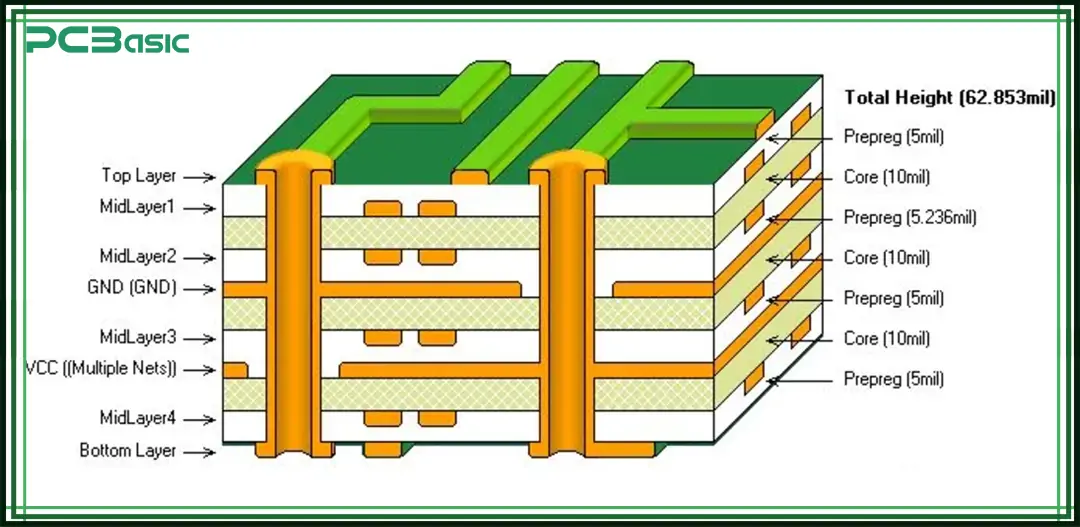
An 8-layer PCB is a circuit board composed of 8 layers of copper and insulating materials pressed together. These layers are connected through vias. Its structure usually includes the signal layer, power layer, ground layer and internal routing layer.
Compared with ordinary circuit boards, the 8-layer PCB allows for more complex routing, helping to design more complex circuits. It can also make signal transmission more stable and have stronger anti-interference ability.
The 8-layer PCB is particularly suitable for high-speed electronic devices with high-performance requirements, such as servers, medical instruments and communication systems.
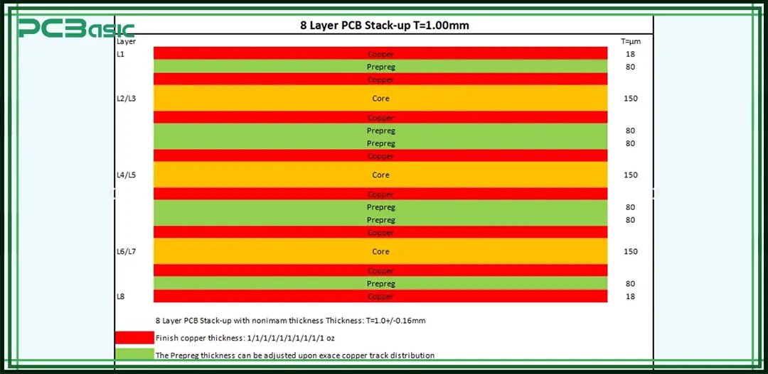
The 8-layer PCB stack-up structure refers to how the layers inside the PCB are arranged and what each layer is used for. Different PCB stack-up structures will directly affect the performance of the circuit board, such as whether the signal will be interfered with, whether the power supply is stable, or if the board will heat up severely, etc.
Choosing the right 8-layer PCB stack-up structure can make your PCB signal more stable, enhance its anti-interference ability, and improve power supply efficiency. The following are several common 8-layer PCB stack-ups and in which scenarios they are suitable for use:
1. Signal / Ground / Signal / Power / Ground / Signal / Ground / Signal
• Best for designs with high signal integrity requirements, such as high-speed communication and server motherboards.
• Benefits: Low interference, stable signals, ideal for high-speed circuits.
2. Signal / Ground / Signal / Power / Power / Signal / Ground / Signal
• Suitable for high-speed circuits, such as high-performance processor boards.
• Dual power layers provide sufficient current, while two ground layers help reduce noise, ensuring stable operation.
3. Signal / Signal / Ground / Signal / Signal / Power / Ground / Signal
• Ideal for mixed-signal devices (analog + digital), such as audio processing boards.
• The middle ground layer separates analog and digital signals, preventing crosstalk.
4. Signal / Ground / Signal / Signal / Signal / Ground / Power / Signal
• Best for wireless or RF devices, such as Bluetooth/Wi-Fi modules.
• Multiple ground layers enhance shielding, reduce signal interference, and improve high-frequency signal clarity.
5. Signal / Power / Ground / Signal / Signal / Ground / Power / Signal
• Suitable for high-speed digital circuits.
• Alternating power and ground layers isolate noise and improve signal integrity.
6. Signal / Ground / Power / Signal / Signal / Power / Ground / Signal
• Provides flexible routing space and balanced power distribution.
• Ideal for control boards requiring multiple functional modules.
Simply speaking, different 8-layer PCB stack-ups are suitable for different uses. Whether you are doing high-speed signals, a mixture of analog and digital, or wireless communication, the stack-up structures are all different. Choosing the right structure makes your 8-layer PCB more stable, the signal cleaner and the operation more reliable. When designing, it is essential to select the most suitable stack-up structure based on specific requirements.
The standard PCB thickness of an 8-layer PCB usually ranges from 1.6mm (63 mil) to 2.4mm (94 mil), depending on the copper foil thickness and the choice of prepreg/core material. However, the final thickness may also be affected by the following factors:
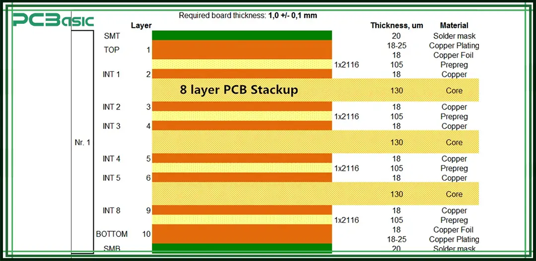
• Copper thickness (e.g., 1 oz, 2 oz)
• Dielectric layer spacing
• Material types used in the PCB stack-up
Thicker PCBs have better strength and are less likely to bend, making them suitable for industrial equipment, while thinner PCBs are more suitable for small-sized devices, such as mobile phones or portable devices.
In the actual design, the standard PCB thickness needs to be determined based on the characteristics of the circuit, such as whether to control the impedance, whether there is a heat dissipation requirement, and the production capacity of the factory. Appropriate thickness can also ensure that the PCB can be smoothly installed into the casing and connected to the connector without affecting the product assembly.
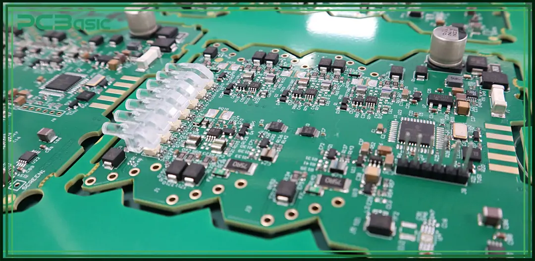
When designing an 8-layer PCB, in addition to meeting functional requirements, it's essential to comprehensively consider electrical performance, structural stability, and manufacturing processes. An excellent design must not only perform well but also be manufacturable, assemblable, and durable.
Here are some key design recommendations:
1. Layer Arrangement:
A well-planned 8-layer PCB stack-up ensures proper distribution of signal, power, and ground layers, optimizing routing efficiency and overall performance.
2. Impedance Control:
For high-speed signals, trace impedance must be strictly matched. It's recommended to use simulation tools combined with the specific PCB stack-up to accurately calculate trace width and spacing, ensuring signal integrity.
3. Structural Symmetry:
Maintaining symmetry between the upper and lower PCB layers helps prevent warping or deformation during lamination, improving the mechanical strength of the final product.
4. Via Design:
Proper use of through-holes, blind vias, or buried vias according to spatial and electrical requirements can optimize routing efficiency and reduce signal interference.
5. Thermal Management:
High-density routing and high-power components can lead to localized overheating. Therefore, effective heat dissipation paths must be designed, such as adding thermal copper layers or incorporating thermal vias.
6. Material Selection:
For applications requiring high-speed or high-frequency signals, prioritize materials with low dielectric loss and stable performance.
7. Manufacturing Tolerances:
Sufficient production tolerances must be reserved in the design to ensure key parameters like standard PCB thickness align with factory capabilities and quality standards.
By implementing these measures, an 8-layer PCB can achieve a good balance between functionality, reliability, and manufacturability, ultimately ensuring optimal product performance and quality.
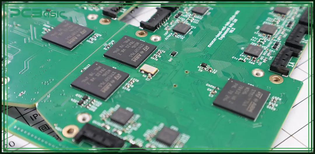
The manufacturing of an 8-layer PCB involves sequential lamination of multiple PCB layers under heat and pressure. Key steps include:
1. Core and prepreg preparation
2. Inner layer imaging and etching
3. Layer stacking and lamination
4. Drilling and via plating
5. Outer layer imaging and etching
6. Surface finish, solder mask, and silkscreen
7. Electrical testing and quality inspection
Maintaining tight process control during manufacturing is essential to preserve the integrity of the PCB stack-up, especially when using advanced materials or fine-line features.
The 8-layer PCB is an ideal choice for high-performance electronic systems. Through a reasonable design of the 8-layer PCB stack-up structure, strict control of the standard PCB thickness, and optimization of the overall PCB stack-up structure, the stability and performance of the product can be significantly improved.
Whether you're developing medical electronics, industrial control systems, or networking equipment, mastering the design and manufacturing of 8-layer PCBs will give your project a technical edge.

Assembly Enquiry
Instant Quote
Phone contact

+86-755-27218592
In addition, we've prepared a Help Center. We recommend checking it before reaching out, as your question and its answer may already be clearly explained there.
Wechat Support

In addition, we've prepared a Help Center. We recommend checking it before reaching out, as your question and its answer may already be clearly explained there.
WhatsApp Support

In addition, we've prepared a Help Center. We recommend checking it before reaching out, as your question and its answer may already be clearly explained there.